Protecting Your PCB Design From Machine Assembly Defects

These days, most PCBs are not hand assembled, save for specialty components or in order to eliminate a reflow pass. When you get a board assembled on an automated line instead of manual labor, you expect your PCBA to be free of defects. In reality, no PCB assembly process is ever perfect, even with top-of-the-line equipment, and a small percentage of your boards might occasionally face quality issues. However, being aware of issues can help you optimize your design to minimize or even prevent some common PCB assembly defects.
PCB Assembly Defects
There are many defects that can arise in any PCBA, both during fabrication and assembly. Some basic DFM practices from a designer, and a DFM review from your fabricator, will . Although the probability of seeing these defects is generally low, you're statistically guaranteed to see defects if enough boards are put through production. The list of some of the main PCB assembly defects is shown here,
1. Solder Bridges
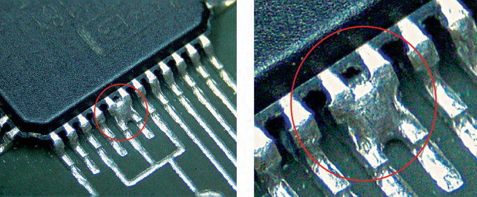
One of the most PCB assembly defects that could cause serious damage when powered up is solder bridges or shorts between the leads of fine pitch components. Shorts are usually tiny and easily escape visual inspection. Shorts during PCB assembly can be caused by various factors. For instance, component pads that are too wide with little gap between them can result in solder bridges. Shorts can also be caused by excessive amount of solder placed on the pads due to excessively thick stencils, or possibly dirty stencils.

Solder bridge defect identified visually. [Source: Springer]
2. Open Joints
Open joints result from insufficient solder, or possibly from lifting of components during soldering (see tombstoning below). Unless you’re using a magnifier, some open joints on a PCB pad are almost impossible to detect. A visual check will indicate whether all the surface mounted components are properly soldered. However, even a tiny gap between the component lead and the solder pad is enough to prevent the electronics from functioning correctly. In addition, a stencil that is too thin can also cause lesser solder paste to be deposited and hence the open joints. While they can be tough to identify visually, open joints will generally read as high resistance with a DMM. This gives a simple way to verify what would be suspected as an open joint.
3. Floating SMD Components
Through-hole components can be held in place by their own weight and gripping from the leads poking into the through-holes. This is not the case with SMD pads; these parts essentially sit on top of solder paste before passing into reflow. The quantity of solder paste on the pads and the temperature difference across component pads can lead to two problems:
- Floating parts that experience skew
- Insufficient wetting on one pad, leading to tombstoning
- Vibration of the PCB as it passes into reflow
If the solder wets on both sides of the part within a relatively small time difference, then we should not expect skewed parts or tombstoning. However, excessive solder on one pad or uneven wetting will both produce skew and/or tombstoning. This is known to cause skew in SMD passives, testpoint pins, DPAKs, SOTs, and other flat SMD packages with small lead count.
Shifting of a component due to poor wetting and low temperature on component pads. [Source].
While the possibility of component shifts in PCB assembly is low, they do happen and are usually obvious to the careful eye, except with packages like ball grid array (BGA) where the leads are at the bottom of the component. A rework to realign the component requires desoldering the component and manually soldering it again. This may cause further quality issues as the success of these tasks depends on the skills of the technician. Component shifts are usually caused by physical factors such as bent leads or high vibrations in the conveyor.
4. BGA-Specific Defects
BGAs can have their own specific set of defects that will arise during soldering. These are related to soldering temperature, quantity of printed solder paste, flux outgassing, and reflow profile during soldering. The list of defects includes:
- Head-in-pillow
- Insufficient wetting
- Excess or insufficient solder paste
- Leftover flux or uncured no-clean flux contamination below the BGA
These defects can lead to intermittent failures (namely head-in-pillow or insufficient wetting) during thermal expansion or cycling. This might appear to present as an intermittent failure from fractured traces below the interconnect, but it is actually in the solder ball above the PCB. The other factor here relates to cleanliness of the BGA soldering region, where breakdown of uncured flux can occur over time, leading to potential ECM from active components in leftover flux, including in uncured no-clean flux. This issue with no-clean flux is one reason to potentially extend the reflow time, or opt for a cleaning procedure that can remove all residues from no-clean flux.
In cases where BGAs fail to solder properly, you will only be able to notice very severe defects like shifting (floating) and lifting from the pads. These defects are very uncommon, and more often won't notice the more common defects without X-ray inspection of the BGA. X-ray inspection provides a direct view of the solder balls and allows identification of solder ball bridging, head-in-pillow, excess solder, or insufficient solder (opens). Even more difficult to diagnose is intermittent failures from fractured microvia-in-pad being bonded to BGA solder balls; this has to be identified in electrical testing and is an important part of microvia reliability.
5. Warpage
Board warping can occur due to incorrect design of the stackup or processing factors during assembly. When warpage is excessive, the board could violate flatness (bow and twist) standards on the finished PCB as specified in IPC standards. Typical allowed values of warpage (bow and twist) are less than 1.5% for through-hole-only boards, or less than 0.75% for boards with SMD parts. The various factors causing warpage include:
- Mixed orientation of boards in a panel:
- Large CTE and Tg mismatches in the stackup
- Asymmetric stackups
- Repeated reflow and wave passes
- Oven temperature profile drift
This is as much a design problem as it is an assembly processing problem. Designs that are optimized for minimal reflow passes will eliminate one common source of PCB warpage.
How to Spot PCB Assembly Defects
PCB assembly houses generally include some minimum level of equipment to maintain tooling, inspect assembled boards, and perform rework. Inspection levels vary by assembly house capability, as well as by level of service being provided by the assembly house. However, in general, the assembly house should have one or more of the following capabilities for inspecting PCB assemblies for defects.
1. Visual/Computer Vision Inspection
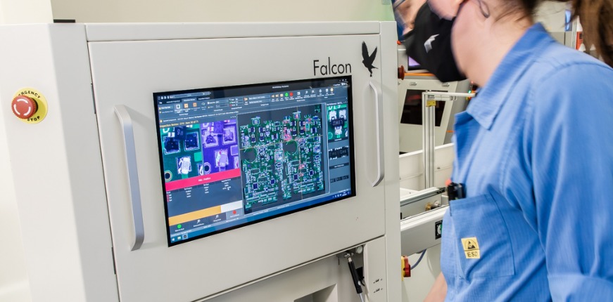
Visual inspection can be performed manually by an assembly operator, but more often this is automated and will be performed with a specialized automated optical inspection (AOI) system. AOI systems are computer vision systems that can pick out placement errors, soldering defects, opens, surface damage, and discoloration that could be due to contamination. Any defect or suspected defect is then flagged for an operator, who will perform a manual visual inspection.
More advanced visual inspection falls into three possible areas:
- Machine learning assisted visual scans, where a computer
- X-ray inspection, possibly also assisted by machine learning
- Computed tomography (CT) scans, which produce a 3D image of the interior of the board
The cost of AOI systems has come down and most PCB assembly houses will have these systems in place. X-ray inspection will be needed for quality control in BGA assembly. Finally, CT scans as applied to PCB inspection ranks among the most advanced computer vision inspection modality and is not available at all manufacturers. Don't assume which capabilities your assembler has available; make sure they have the capabilities you need to ensure your defect rate target can be hit and that they can implement the right quality control procedures for your PCBA.

2. Surface Chemical Testing
If you look at the list of above defects, you will notice that a few of these are related to cleanliness of the assembled PCB; leftover flux residues were mentioned specifically. Visual inspection is focused more on solder, placement, and surface defects in the PCBA, but chemical testing can be performed to identify contamination. There are many chemicals used throughout PCB fabrication and assembly processes, and some of these can leave behind contaminants that create a challenge for long-term reliability of the assembled PCB. Some of the standard chemical test for cleanliness and contamination analysis include:
- Surface insulation resistance
- Ion chromatography
- Resistivity of solvent extract (ROSE)
As a designer, you can certainly come up with cleanliness requirements that you will accept, and these can be included in the notes on your assembly drawing. The other option is to state that board cleanliness must conform to a particular standard, generally IPC-610 or IPC-J-STD-001. If there is some other relevant industry standard that should be a conformance target, then this should be specified. Some of these cleanliness and defect conformance targets can be found in aerospace, automotive, and medical industries.
Whenever you’re ready to export your finished design and prepare documentation for volume production, make sure you use the design and analysis tools in Altium Designer®. The Draftsman extension gives you the ability to quickly create fabrication drawings, complete with assembly notes in standardized formats. When you’ve finished your design, and you want to release files to your manufacturer, the Altium 365™ platform makes it easy to collaborate and share your projects.
We have only scratched the surface of what’s possible with Altium Designer on Altium 365. Start your free trial of Altium Designer + Altium 365 today.


