


Flex Circuit Miniaturization and Biocompatibility with SAP Processes

At a Glance
Fabricators typically purchase flexible laminate, which consists of a layer of rolled annealed or electro-deposited copper on one of both sides of the dielectric. The most common dielectrics are polyimide, LCP, and polyester.


Flexible circuits have been around for decades and are one of the fastest growing segments of the printed circuit board market. I imagine at this point in time, most experienced printed circuit board designers are aware of the benefits of using flexible circuit technology:
- Solves a packaging issue
- Reducing space and weight needed
- Reduced assembly costs
- Facilitates dynamic flexing
- Thermal management
- Improves product aesthetics
- Biocompatibility
- Increased reliability and decreased opportunity for operator error
How to push these advantages even further:
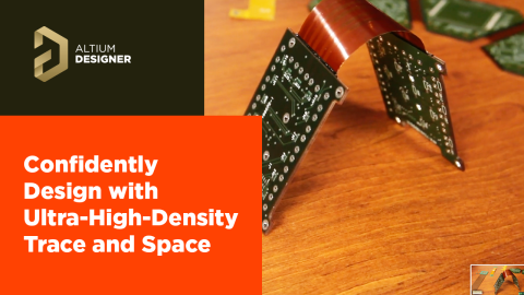
Today, I want to talk about another tool in the toolbox that allows printed circuit board designers to push these advantages even further. I have written several blogs talking about semi-additive PCB processes and the ability to now route trace and space at 25 microns (1 mil) and below. (I’ll include a few links at the end of this blog post). Now, let's apply those benefits specifically to flexible circuit design.
Taking a quick step back, let's review flexible laminates. Fabricators typically purchase flexible laminate, which consists of a layer of rolled annealed or electro-deposited copper on one of both sides of the dielectric. The most common dielectrics are polyimide, LCP, and polyester. Polyimide and LCP are often selected for medical applications.
Printed circuit board fabricators then etch away the unneeded copper forming the desired circuit pattern. That is a grossly over-simplified explanation and I imagine my PCB fabricator friends will be letting me know that! Truth be told, fabricating with flexible materials is much more challenging than with rigid materials. Handling a thin layer of flexible material requires specialized processes and tight process control. As a result, designers are typically limited to a 75-micron (3-mil) trace and space and at some fabricators, even the 75-micron feature sizes are a cost adder.
What if you could push that feature size limit to 25 microns, or even below?
Today, fabricators now have the option to run semi-additive processes, and one particular process, the A-SAP™ process has specific advantages to the medical market. The A-SAP™ process also starts with a copper-clad laminate, but the first step is to completely remove the copper. A thin layer of electroless copper is then applied, the photoresist is applied and patterned, the trace patterns are then electrolytically plated, the photoresist is stripped, and the electroless copper is then etched away leaving the desired circuit pattern. The significant result of this process is that PCB fabricators can now provide flexible circuits with feature sizes of 25 or even 15 microns depending on their equipment set.
This process allows printed circuit designers to push the advantages of flexible circuits even further, specifically when looking at reducing space and weight and biocompatibility.
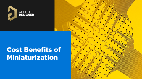
Reducing space and weight can be looked at a number of ways. The first thing that likely comes to mind is reducing the overall footprint of the flexible circuit. Routing with even 25-micron lines is a significant change from the 75 microns we are designing with today and could potentially shrink the circuit to 1/3 of its current size. Of course, we also have to factor in vias, etc., that won’t be reduced, but even with that factored in the impact is significant.
A second consideration is an ability to reduce layer count. In some applications, rather than having an overall size reduction be the primary driver, the ability to route with these ultra-high-density features allows the PCB designer to reduce the overall number of layers which can have a significant benefit to the weight and flexibility of a design.
Yet one other way to consider applying these feature sizes is to consider the opportunity to add more functionality within the existing footprint. There are a lot of options to consider!
Switching focus to biocompatibility, once the copper laminate is removed, the printed circuit board fabricator is no longer limited to just copper as a conductor. The conductive metal could be gold, platinum or other noble metals. The benefit of this being a much more biocompatible solution than has previously been available. Polyimide and LCP are both excellent choices for biocompatibility and are regularly used for that reason in both medical and wearable applications. Both materials have been tested with gold and platinum conductors and this combination is being readily adopted by the medical market.
These new fabrication techniques are changing the way PCB designers look at solving complex design issues. If you are interested in learning more about SAP processes, please refer to a few of our previous blogs. We have gone through the basics to SAP processing, and recently looked at some of the top questions related to the printed circuit board stack-up; explored some of the “design rules” or “design guidelines” that do not change when designing with these ultra-high-density feature sizes; and explored the design space around the possibility of utilizing these ultra-high density circuit trace widths in the BGA escape regions and wider traces in the routing field. The benefit is a reduction in circuit layers and the concern is maintaining 50-ohm impedance. Eric Bogatin recently published a white paper analyzing just this benefit and concern.
About Author
Related Resources
Design to Release, Without the Friction
- Keep reviews tied to the right version
- Reduce handoff confusion and rework
- Spot sourcing and release risk earlier
- Work solo, share when needed
Get Started
Thank you, you are now subscribed to updates.


