A Big Kick in PCB Interconnect Solutions: Multi-Board Best Practices
I’ve always enjoyed thinking about circuits similar to tiny cities. Copper routing as the streets, components as building structures, vias, and the following electrons as the inhabitants running around. But imagine what PCB would be in the city from Inception where the flat ground starts turning on its head and extending overtop, or if Salvador Dali became a city planner.
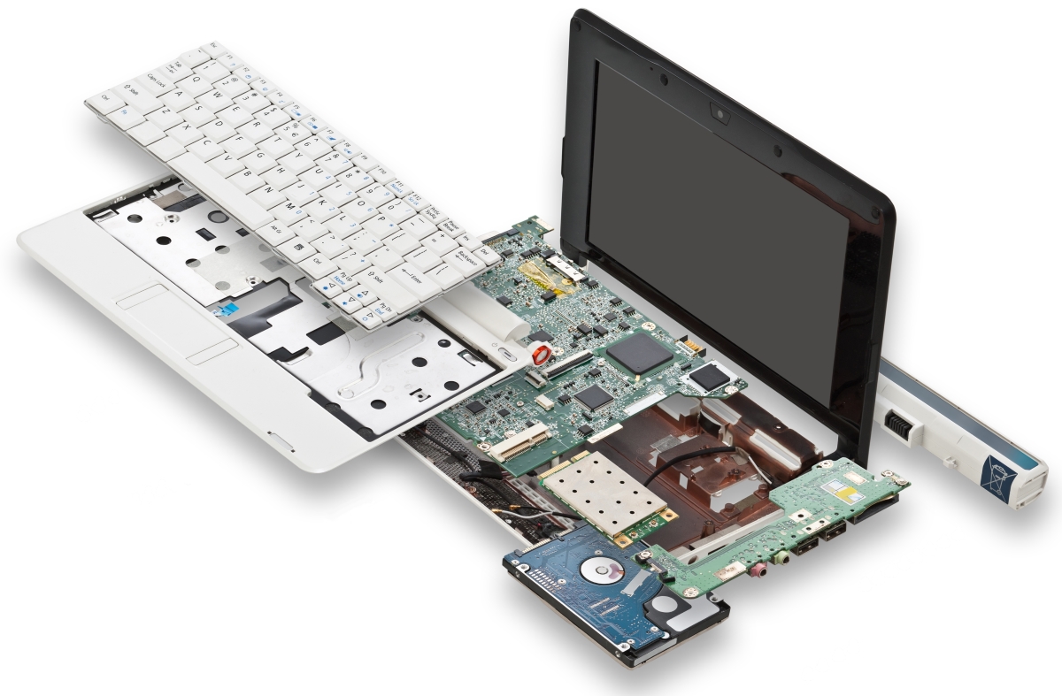
In today’s world of densely packed components (HDI), advanced manufacturing capabilities, and wonky product shapes, you may find yourself at a loss for horizontal real estate and looking into vertical space. More specifically, you may come across a situation in which you need to separate your printed circuit board into two, three, or even twelve HDI boards. The beauty of your PCB city comes in when you can start producing a multi-board PCB design.
Whether it be your consideration of space within a product or keeping signals isolated from one another, you’ll likely need your boards to talk to each other. Enter PCB interconnection: the practice of running physical, non-printed cables between multiple printed boards in order to achieve a fully connected circuit. With the city laid out (and a three-hour break for Inception), we can know more about the situations requiring our multi-board PCB cities to bend and stack.
First PCB Interconnect Solution: How’s it Look?
Some of the more common PCB stacking techniques involve a vertical stack, one on top of another. This is personally my favorite method to see implemented as the final product has the potential to look like a skyscraper with floors as PCBs. What PCB city is complete without PCB skyscrapers?
When stacking any boards, similar to designing a single PCB, you’ll need to take care of the orientation of signal lines that are running through. Crosstalk, impedance discontinuities, and electromagnetic emissions are real issues that will bite you if you do not pay heed. To mitigate these issues, here are some quick tips to incorporate into your considerations:
-
All signal layers should be adjacent and closely coupled to an uninterrupted reference plane.
-
Reduce AC impedance at the top end and dramatically reduce electromagnetic radiation with closely-coupled planes.
-
Further, reduce radiation by routing high-speed signals between the planes.
In addition to these tips, you’ll also need to appreciate the space that comes with the physical, non-printed connector cables or pins that will connect your boards together.
Designing for Manufacturing and Serviceability
Just with any design, you’ll want to make sure you plan out your board for its full livelihood: will your design be lasting years or decades? How often will your board require updating and maintenance? Maintaining strong communication with your manufacturer will allow you to keep your design working far into the future. When in search of manufacturing facilities, ensure you do your due diligence and attain their limitations and requirements for manufacturing.
Space requirements needed to manufacture your product will need to be kept in mind. In addition, if your product is maintained regularly or if your product breaks but is designed for repair, then the physical space required to carry out such procedures should also be understood and designed for such. Again, don’t forget about the PCB connector cables that may or may not run between the boards.
Ensuring Your PCB Doesn’t Collapse
Often an afterthought, testing procedures of your PCB design will, of course, need to be implemented at some point if you are to keep any amount of quality assurance in your flow. From producing prototypes to testing in various conditions to determine any potential overlooked design flaws to using your software tools to simulate and run consistent, reliable testing on rule checking as well as product analysis, your PCB tests need to be implemented.
Testing procedures involving the use of probing can be a physical challenge when you are vertically stacked PCB. Keeping in mind the space requirements of not just your product’s chassis, but your testing apparatus too will be a crucial step when it comes time to test. It’s like trying to make a sandwich out of your PCB city with PCB skyscrapers—you have to prepare it properly.
A Butter Knife Won’t Cut a Tree, Use the Right Software
While your PCB multi-board can be done, painstakingly, with tools as primitive as a pencil and paper; you’re going to want to utilize the design software which can make your process smooth and intuitive. After all, the software is something that you’ll be working on the majority of the time in your designs—why shouldn’t you be using software that you both like and find incredibly helpful?
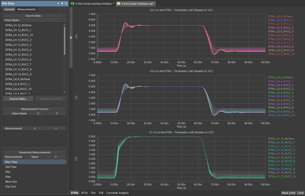
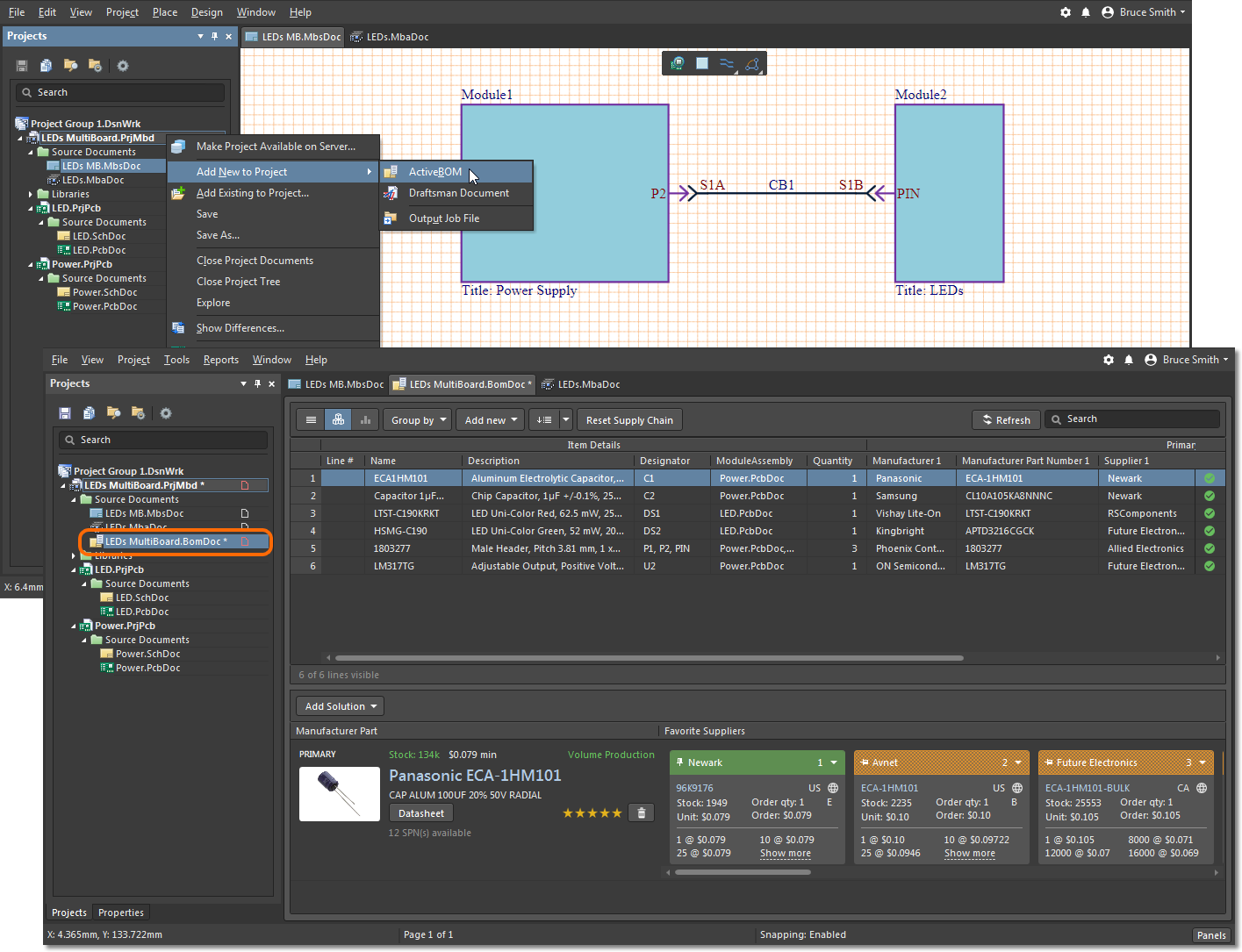
For multi-board systems specifically, I find using software that has features like multi-board PCB signal analysis can be extremely beneficial. Your design as a whole will be acting as a single PCB, so being able to properly analyze the separately communicating parts as a single PCB will be critical to maintaining your product’s integrity. Furthermore, 3D visualization capabilities also assist when determining the physical stacking of your boards.
Multi-Board PCB Designs Aren’t Your Enemy
Without over-thinking the process, designing Multi-board PCBs with interconnects is a fantastic solution for overcoming space requirements, isolating signals, or simply making your design look as cool as you imagine. By keeping in mind the purposes and utilities of a multi-board system, as well as understanding the full effect of your PCB design software on your capability for smooth layout, you’ll be able to build your PCB city in no time.
With the software tools listed above all wrapped into one unified design environment, Altium Designer will empower you to smooth out your design and keep your city looking like Manhattan instead of Inception. After all, the goal for your PCB software is to make your design process as intuitive as it can be, with as little time spent outside of the software and consulting other tools and services as possible.
If you would like to discuss how Altium Designer can assist in your PCB interconnected multi-board design, talk to an Altium Designer expert today.


