PCB Design for Electromagnetic Compatibility


Whether it's a video for Altium Academy or an engagement from a consulting client, I get asked to review a ton of designs. Some of these designs are from students or startup founders, and some come from big companies trying to push a new product to market. There's one thing that binds them all together, especially when a design is intended for sale to customers at volume. That thing is a requirement for low EMI and for EMC compliance.
EMC testing refers to a set of electromagnetic emissions tests performed at the system level, with different test requirements for different types of designs. The system level refers to everything that goes into the product (cables, enclosure, specialty materials, mechanical elements, and additional modules). However, electromagnetic compatibility begins in the PCB because this is where components connect to each other and where circuits are formed. Everything around electromagnetic compatibility relates in some way to your PCB design decisions, so make sure to fully understand the factors that influence EMC in your design by reading this article.
Where the Pros Hunt for EMI Problems
Electromagnetic compatibility is such a broad area of testing that many engineers have dedicated their careers to it. This includes some of our guests on the Altium podcast, and they will tell you that the circuit board is a prime location for the origination of EMI problems.
There are common areas where EMI can be observed, which just so happen to be the observation points in standard EMC tests:
- Conducted emissions over cables
- Conducted emissions over connectors
- Conducted emissions via metal in an enclosure
- Radiated emissions from PCB components or circuits
- Radiated emissions from areas without ground
- Radiated emissions from board edge features
- ESD propagating current through unintended parts of the board
- Created emissions from strong transients
- Noise coupling between floating bits of metal, leading to high-frequency radiation
Obviously, this is a broad set of issues that can create problems with EMI and a resulting EMC test failure, but not all are solved directly on the PCB. However, when the PCB is designed appropriately, it makes implementing a solution to many of these problems much easier, or the solution will be built in and chances of passing testing will be much higher.
Foundational PCB Design Practices Ensuring Electromagnetic Compatibility
There are a few EMC design tips that will apply to just about any electronic device and should form the basis for modern electronics design. No, this does not involve copious use of ferrites; it starts earlier when planning out the structure of your board and placement of components.
It Starts in the PCB Stackup
Inside your PCB stackup are plane layers and signal layers, and the arrangement of these layers is one of the big determinants of EMI susceptibility in your PCB layout. The arrangement of plane and signal layers also determines performance in two areas related to EMI: signal integrity and power integrity. Whether the mechanism lies in signal integrity, power integrity, or failure to contain noise in general, the stackup also determines EMI generation and radiation into free space.
For this reason, all modern designs should have a well-defined ground, whether as a plane or as a copper pour region. Because most modern designs involving a visual processor start on a four-layer board, you should start with one of the standard arrangements with a four-layer stackup, usually SIG/GND/GND/SIG.

4-layer stackups require planes to ensure low radiated EMI and high shielding effectiveness.
This GND-SIG pairing of layers extends to higher layer counts and is the primary strategy that should be used to ensure low EMI susceptibility and emissions.
In the case of two-layer boards, you can use a ground plane on one side of the board while having components mounted on the other side. Many two-layer boards go beyond this and have component placements on both sides of the PCB, as well as routing. This is an instance where copper pour is brought up by new designers as the key to passing EMI tests.
In some sense, those new designers are correct. The copper fill defines ground for signals in the design, and so it plays the role of a ground plane to an extent. However, when you get to a situation where the copper fill density is very low, there will be many signals that do not have a well-defined ground and which will radiate strongly. At this point, you must go to a four-layer board in order to ensure low EMI susceptibility and emissions.
Routing Signals and Power Rails
Where you route these two elements will be a big determinant of EMI, both radiated and received. Traces and rails in power circuits can carry switching signals which transfer between extreme voltage values. Traces can also carry switching signals, and modern digital components can switch the signals at fast edge rates (low rise time). The EMI that can be generated from switching power and switching signals is proportional to:
Rise time = ΔV/Δt
Digital signals and switching regulators will contain the highest switching rates on your PCB, so they require the most attention to routing. Route these only over continuous ground, do not attempt to route these over splits in the ground plane. In fact, do not include any splits in power or ground unless your system is designed to be galvanically isolated.
Design for galvanic isolation comes up in the context of isolated DC/DC converters, but these circuits do not actually route conductors over splits in the ground plane. Instead, they use magnetic induction to transfer power between two regions with separate grounds. In this case, digital signals, which typically originate on the secondary side from a lower voltage, need to stay on the secondary side, and the same principle still holds: don't route over a gap in the ground plane.

This snapshot from my Dual ADC Module project shows how to handle galvanically isolated regions: don't route copper between them!
By keeping signals, power rails, and switching circuits closer to ground, you help reduce radiated EMI as well as reduce some signal integrity problems, most notably crosstalk.
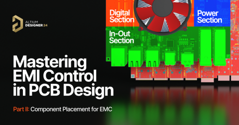
Component Placement Helps Suppress Radiated EMI
The PCB stackup is like a foundation for a new building: the success of your routing and placements relies on getting your stackup correct. Stackup design and routing help address one important set of EMI issues, but placement is also very important. Some circuits rely heavily on placement in that parts placement determines their noise profile.
Which circuits and components rely the most on precise placement? In some sense, the answer is "everything," as each circuit and its main component should be laid out in very tight functional blocks. We can come up with several examples where spreading out your placement too much creates a large amount of noise:
- Switching regulators
- Oscillators or crystals
- PWM generators
- Motor drive circuits
- Digital processors and their I/Os
Putting each piece of these circuits as a functional block, and connecting them together with the required power and signals, is one way to create a functional layout that also reduces noise, particularly from switching circuits.
The physical mechanism by which this works is the reduction of loop area where a switching waveform exists. This is one reason why we tend to tell designers to layout switching regulator circuits with very tight component placement and minimal loop area. This reduces the size of the current path and thus the magnetic flux from these current loops.
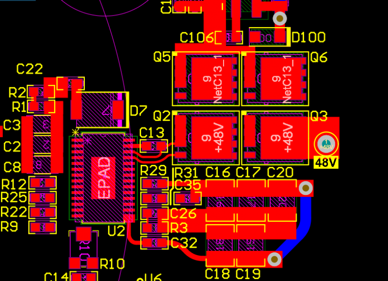
Switching regulator layout should have tight routing in order to reduce EMI from switching circuits.
Next, when placing each circuit in the PCB, keep components in each circuit together and define their own regions on the board only for these circuits. This is one reason it's a good idea to separate each circuit into its own sheet; it helps you keep track of each functional block in the PCB. In the example below, we can identify several different circuit blocks that are clustered around specific components which perform the primary function in each circuit. This helps you keep a well-organized, highly logical layout where each block tends to exhibit minimal EMI, and this is particularly true for switching regulators. This is also a necessary layout style for digital ASICs and large digital processors, where the supporting decoupling/bypass capacitors are placed close to the components to ensure minimal current loops.
PCB layout provided by Sadek Kanaan in our 1-minute design review series on Altium Academy. The boxes show component groups placed on the top layer; this placement helps keep current loops small and thus helps reduce EMI.
Connector Pinout Design and Filtering
PCBs don't exist in isolation; they need to connect to something else in order to perform their job. This could be a connection to a power source, another PCB that exchanges data, a wireless connection, or some other electrical device. This means some kind of connectors will be present in the design, and these connectors will influence EMC.
Connectors play a role in determining radiated emissions and EMI susceptibility through their pinout and based on the connection (power or signal) they are carrying into the board. Because of this, some designers will default to shielded cables when they are not needed, or they will use customized board-level shielding to reduce radiated emissions from components. Sometimes these are necessary, but ensuring EMC starts with designing an appropriate pinout for signals traversing connectors.
Just as was the case with ensuring ground is near signals on the board, we want to do the same on a connector and cable. This means some of your pins on your connector will need to be allocated to ground.
The allocation of GND pins in this Micro-D connector might result in radiated EMI from the GPIOs on the left side of the pinout. This EMI would be measured from the cable.
These ground pins will provide a reference for signals that move across the conductor, and thus their presence will help to reduce radiated emissions. In the high-speed domain, we tend to worry less about the emissions because wiring on these cables will be differential. In this case, we do worry about differential crosstalk, and this is one reason to include ground pins on the connector interface.
For other interfaces, namely low-speed digital, DC configuration, and power, we may need filtering going in and out of the board to reduce conducted emissions. Conducted EMI coming into the board typically comes from the power section; wall outlet connectors also carry noise which is seen as conducted and radiated EMI. To deal with these noise problems, some filters are available that can provide high attenuation in specific frequency ranges:
- Common mode chokes
- Differential mode chokes
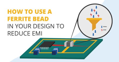
- Ferrite line filters
- Passive filter circuits
- High-frequency passives for filtering
Simulate and Test
Whenever you're using a filter circuit, or if you apply things like board-level shielding and enclosure-level shielding, consider pre-compliance testing to ensure your design will perform to standards. When filter designs are used and switching circuits are developed, simulations can be helpful as they give you an idea of what to expect in experiments. Testing could involve pre-compliance testing, something which is recommended to help identify major EMI problems before paying for certification testing at an EMC test lab.
Whether you need to build reliable power electronics or advanced digital systems, use the complete set of PCB design features and world-class CAD tools in Altium Designer®. To implement collaboration in today’s cross-disciplinary environment, innovative companies are using the Altium 365™ platform to easily share design data and put projects into manufacturing.
We have only scratched the surface of what’s possible with Altium Designer on Altium 365. Start your free trial of Altium Designer + Altium 365 today.

