How to Create a PCB Panel Fabrication Drawing in Draftsman

At a Glance
Not all designers will create their own PCB panels, but if you’ve been asked to do this you can use the built-in drawing features in Altium Designer.


PCB panels need a fabrication drawing, just like any other PCB that will go into production. Individual PCB fabrication drawings only show drills and board features for a single PCB, but these need to be consolidated into a single drawing for the entire panel. Depending on the company or manufacturer, some design teams need to take over creation of the panel drawing, including specifying depanelization method and arrangement of boards in the panel.
If your design team will create a panel, you can use a complete set of native design tools in Altium Designer. Another option is to export the panel drawing into another program (most commonly AutoCAD) in order to finish the panel in a custom format or compile it with other data (such as mechanicals). Here’s how you can create your drawing format and export the required panel drawing in Altium Designer.
Getting Started With Panel Fabrication Drawings
In this article, I will show an example project which was provided by Zach Peterson. This project is for an LED connector board and it gives a good overview of the panel fabrication drawing creation process.
Before you jump into creating your panel, you should answer some important questions first:
-
How do you plan to depanelize the PCB?
-
When panel sizes does your fabricator support?
-
Have they specified tooling holes and V-score grooving requirements?
-
Do the panels require fiducials?
-
If tab routing is being used in the panel, what is the tool size?
If you can get this information, then you will have enough data to start creating your own panel.
Start the Panel With the Embedded Board Array
Inside Altium Designer, the main tool we want to use to create the panel is the Embedded Board Array. This gives you a starting board arrangement to which you can begin to add tooling holes, dimensions, fiducials, layer number etchings, and silkscreen markings.
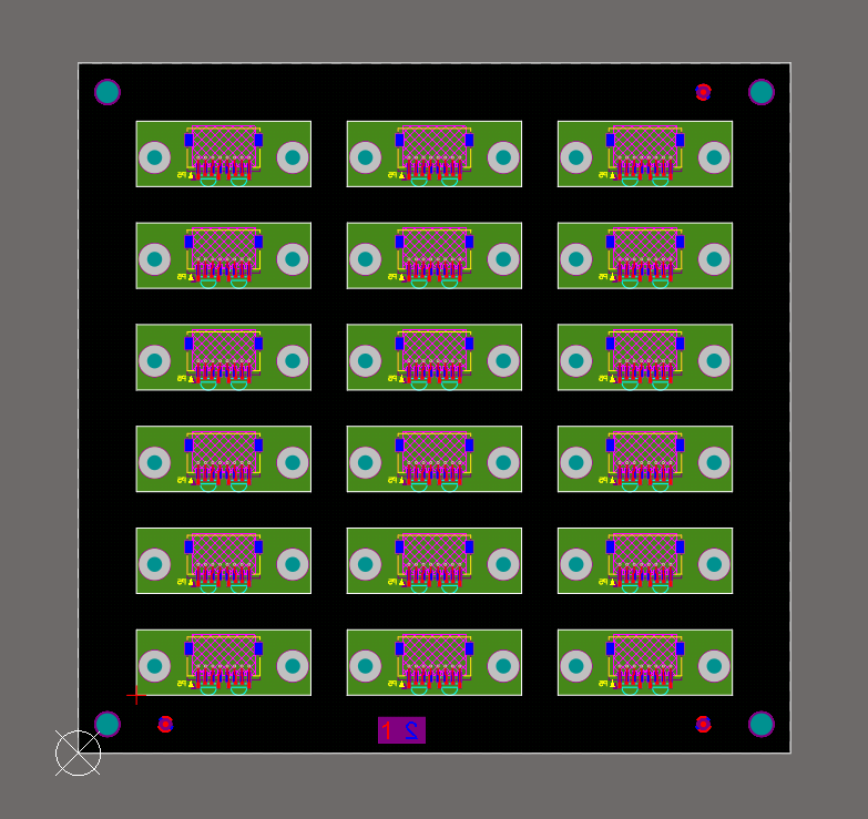
Once the embedded board array object has been placed in the PCB Editor, the locations of any mouse bits or V-scores can be added into the PCB panel. Placing mouse bites involves placing cutouts in the panel and drawing in drill hole spots in the leftover tab regions connecting the boards. This is discussed in this article.
In the example above, we’ll add V-score lines to the PCB to indicate the depanelization lines. Note that V-score lines require some clearance around the tool in order to make room for the V-score blade size and the copper clearance around the board outline. In the example above, there are no planes or pours, so there will be plenty of clearance to any nearby copper or components.
The V-score lines are marked in a mechanical layer as shown below. As we will see momentarily, it can be useful to replicate this into the Drill Drawing layer.
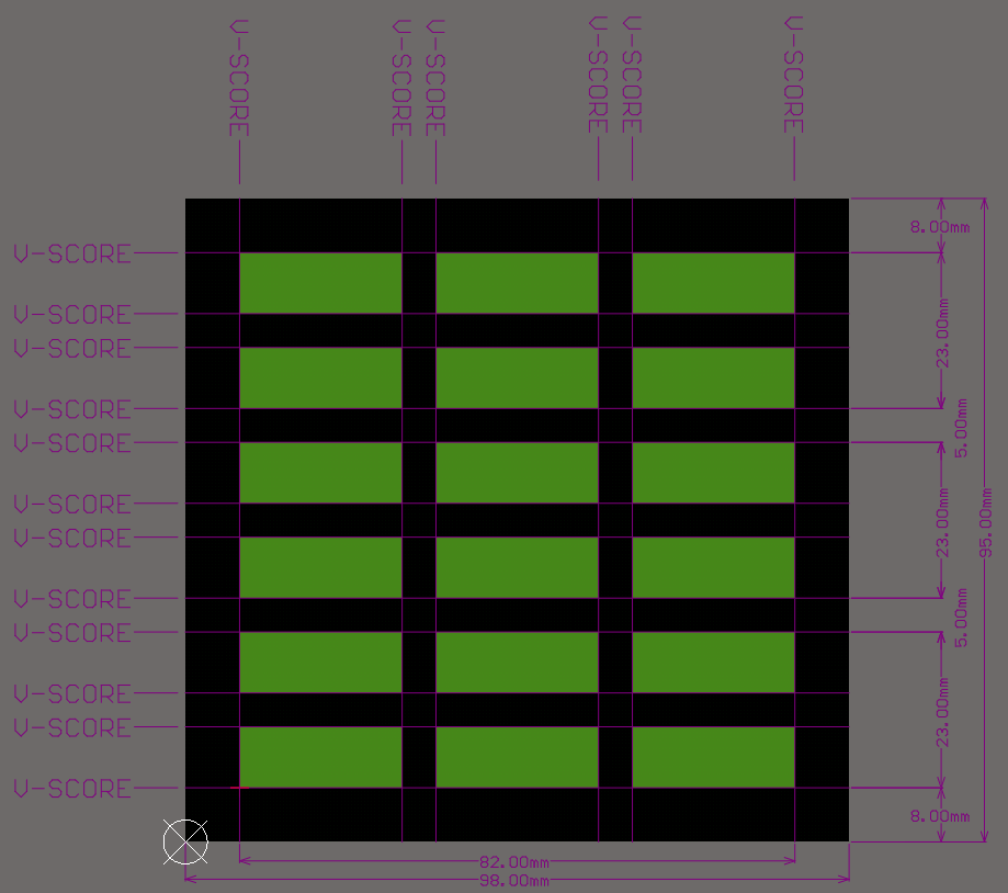
Because the drills from the PCB and the tooling will automatically populate in the Drill Drawing layer, this finishes the fabrication features for the panel. Some manufacturers offer a template (e.g., DXF or DWG file) that can be used to create a panel drawing like that shown above, and this would be imported into a mechanical layer in order to get started.
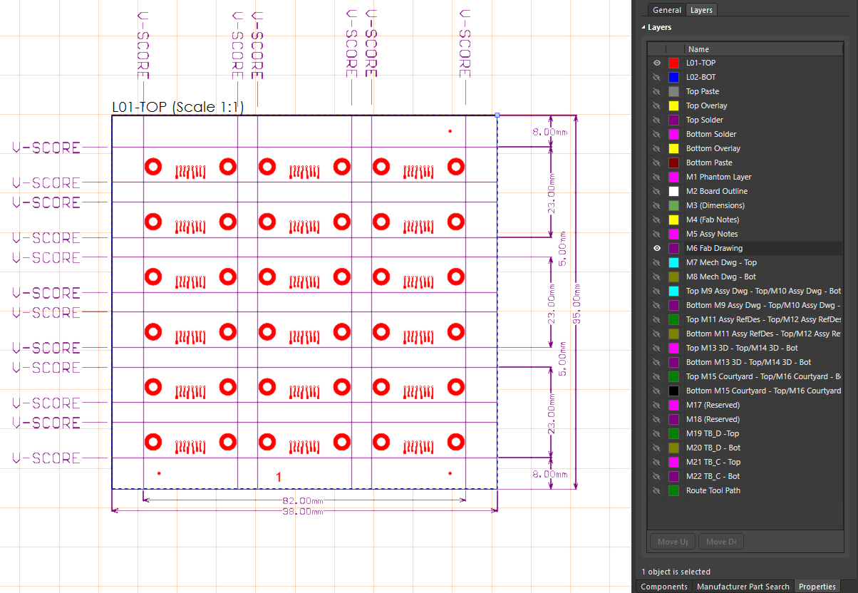
Create the Panel Drawing in Draftsman
Draftsman treats PCB panels just like any other PCB, and various views can be imported into the draftsman drawing. This includes the standard Drill Drawing view, where drill symbols are shown for fabrication, as well as Drill Tables, assembly views, fabrication views, etc.
To get the dimensioned V-scores into the panel fabrication drawing, you can use a board Fabrication View. This will force the V-score lines to show in an isolated view with the Top layer still visible. To do this, place a Fabrication View in the Draftsman document and turn on the Fab Drawing layer. This will show the V-score lines along with the copper in the top etching layer. It’s now clear that you are looking at the panel from the top side with all V-scores clearly marked and dimensioned.
There are still other features that would need to be included in the PCB panel fabrication drawing, including:
-
Stackup drawing showing layers, thicknesses, Dk value or product name, and Gerber layer extension
-
Fabrication notes specifying how the boards will be built and qualified
-
A drill table with clearly marked drill symbols and tolerances
-
Title block with project information, company information, and traceability documentation
-
Any information on controlled impedance requirements on each layer
If you want a consolidated drill view with PCB panel features this is where it helps to copy the dimensioning and V-score lines into the Drill Drawing layer. This allows you to create everything for your panel fabrication drawing using mechanical layers in the PCB Editor.
Doing it All in the PCB Editor
If you’re not a fan of Draftsman or you prefer to do everything in one window, you can still draw out the panel fabrication drawing in the PCB Editor. To do this, you can apply your drawing blocks, panel fab notes, stackup drawing, etc. in mechanical layer and toggle these to be visible in the PCB. Once this is completed, it can still be exported to a consolidated DXF file as outlined above. This is still a common practice by many companies, and the DXF export still allows other disciplines to work in a standard file that contains the PCB data.
Whether you need to build reliable power electronics or advanced digital systems, use the complete set of PCB design features and world-class CAD tools in Altium Designer®. To implement collaboration in today’s cross-disciplinary environment, innovative companies are using the Altium 365™ to easily share design data and put projects into manufacturing.
We have only scratched the surface of what’s possible with Altium Designer on Altium 365. Start your free trial of Altium Designer + Altium 365 today.
About Author
Related Resources


Related Technical Documentation

Thank you, you are now subscribed to updates.


