

PCB Design Review Checklist

At a Glance
It’s essential to check a board for issues before production or prototyping. Here’s an extensive checklist you can adapt or use directly for PCB design review.


At the various companies and organizations I've worked for, there have been a wide variety of procedures for reviewing and approving a PCB design for production. It has been more of a quick look over the board at some of the smaller companies to see if there are any glaringly obvious mistakes, and maybe, if the reviewer remembers, running a design rule check report. Even at larger organizations, there has been a distinct lack of procedure and consistency involved, often because there was simply never enough time to create a procedure with the pace of work and the workload levels of all the relevant staff.
We all know how important it is to check a board for issues before proceeding to production or prototyping. No matter how much effort you put into the design, inevitably, something slips through the gaps. If you do not have a robust list of items to look at before sending off your design files, those issues might still slip through to the board fabricator or assembler.
As we're always operating under such high workloads and pressures to get things done, it can be hard to find the time to generate a procedure or process for reviewing your board's design, as I mentioned above. So, rather than talking in this article about the evils of not checking board designs over, instead, I'm going to make your life easier by providing an extensive PCB checklist you can either adapt or use directly for reviewing each board design. Depending on your board and the technologies used on it, some items on this list may not be relevant - or there may be items missing. While this list is relatively extensive, it's not exhaustive as I've intended it to be the starting point for your own process. Hopefully, saving you from taking hours to come up with your own PCB quality checklist from scratch to needing just a few minutes to add any items as you think of them when you read through my list. Note that some items are repeated with different wording in multiple categories because they are important. Each phase of your PCB design for manufacturing review may have different considerations applied to a particular PCB design checklist item during any discussions.
I'm also not going to detail all the items on the list. If the items are relevant to your product/board, I will hope you either understand the PCB checklist item's implications - or are willing to do some research to aid your understanding. Many of the list items have relevant articles associated with them on this blog, written both by myself and some other industry experts.
Before Submitting Your Board for PCB Design Review
- Check for unrouted nets
- Repour all polygons
- Ensure your board has a complete silkscreen, including:
- Company logo(s)
- Product logo(s)
- Copyright notice
- Warning/Hazard label(s) and Icons
- Connectors are labeled, and pinouts are called out where relevant
- QA/Test block with barcode, blank areas for a serial number, dates, and QA/Test checkmarks
- Board name, print date, and revision number
- If there are designators on the silkscreen, then check:
- Each designator is close to and clearly identifies the associated component
- All designators are only in one or two orientations
- Text size and font will remain legible after the fabrications process
- ICs have pin one clearly marked, i.e., the pin one marker is not located under another component
- Update the PCB from its schematics to ensure the schematic and board are synchronized
- Ensure the design rule report passes with no errors
- Ensure there is a design rule to catch nets with only 1 pin
- Ensure you have the board outline on a mechanical layer that will go to the board fabricator
- Fiducials are present for the assembly and meet these criteria:
- Three board-level fiducials are included as a minimum
- Two fiducials are diagonally opposing each other across all extremely fine-pitch components
- Mounting points have sufficient clearance for the chosen washer and screw head
- If an enclosure model is available, it has been tested against the board to ensure there will be no interference between the enclosure and components
- All components (including mechanical items) have accurate 3D models
Your board should be fully production-ready, as far as you are concerned, before sending it to colleagues for a design review checklist to avoid any nugatory effort on their part.

Your PCB layout should have all the required markings finished, as well as the mounting hole and fiducials shown here. Can you spot the silkscreen error in this image?
Layers
- Check the layer stack and substrate heights meet the fabricator's specifications (or that the fabricator can meet your specifications)
- Check the copper thickness on all layers matches the target fabricator's specifications (or that there is a callout on the documentation layer for the required copper thickness)
- Ensure there is at least one continuous, unbroken ground plane
- If your board has controlled impedance nets, they are correctly set up both on the layer stack and in the design rules
- Check if any keep-out track matches the board shape
- Check any board cutouts or slots used for a keep-out barrier to prevent nets from crossing milled areas
A PCB stackup table that was created as part of your front-end engineering specifications can be helpful here as it gives a visual comparison with the data in your PCB editor. A table provided by your fabrication house or manufacturer is the best resource, such as the example shown below.

Example stackup table for comparison in a PCB design review. Image provided by Zach Peterson/TTM.
Signal Path
- Ensure that the ground plane has sufficient current-carrying vias near connectors, and voltage/return sinks
- If required/relevant, ensure voltage planes and areas have sufficient connection vias for current requirements
- Ensure tracks to reference planes are sufficiently wide for current requirements
- Check there are sufficient quantities of vias for the current-carrying capacity of traces
- Check the minimum track widths for all current-carrying nets are sufficient. Consider if a design rule is required
- Check all ground pins have a via to the ground plane
- Check there is a continuous ground plane within one signal layer of any signal trace
- Check any controlled impedance traces have the correct net rules and impedance profile
- Check differential pair tracks are as close together as possible
- Check differential pair tracks lengths are matched
- Check all high-speed signals are length matched, specifically including:
- DDR
- PCIe
- Ethernet
- LVDS
- HDMI
- USB3+
- MIPI
- Check every signal trace has a constant impedance along its length. If the trace changes layer, its impedance should stay the same
- Check traces longer than 1/6th of the rise or fall time of the signal have been simulated:
- Check termination resistors, or another termination is present to prevent ringing or overshoots
- Check termination resistors are in the relevant locations
- Check long traces that hug other traces that have been simulated for crosstalk
- Check all high-speed traces run over a continuous ground pour
- Ensure that no sensitive nets run under noisy components
- Check that the vias for decoupling capacitors are not shared
- Each decoupling capacitor requires its own via for VCC and for GND direct to reference planes
The xSignals package has features in it that can help automate many of these checks after the PCB layout is finished, but before a more rigorous manual review by the engineering team.
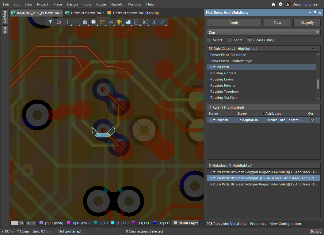
Return path violation highlighted in xSignals. You can choose to ignore this or re-do portions of the routing to eliminate it.
Components
- Check all through-hole pads are set to plated if they are going to be soldered
- Check there is sufficient clearance for the following:
- For pick and place heads in production
- For hand assembly in prototypes
- For soldering pen tip access if any rework is required
- Check bypass capacitors are placed as close to IC power pins as possible (under 15mm)
- Check crystal/oscillator clock sources are as close to the IC clock pins as possible
- Check termination resistors are as close to the signal source as possible
- Check EMI/RFI filtering is as close to the exit point (board edge, connector, shield) as possible
- Check potentiometers increase signal/voltage when turned clockwise
- Check programmable devices have accessible programming header/pads
- Check no high thermal mass components (e.g., large transformers/inductors) are located next to very small components
- Check component placement prioritizes short track lengths for high-speed signals
- Check there are a sufficiently large copper area for heat-sinking high-dissipation devices, including:
- Linear regulators
- Switched-mode power supplies (including LED drivers)
- High power LEDs
- High-frequency gate drivers
- MOSFETs
- Motor drivers
- Chargers
- High-speed microprocessors
- Power amplifiers
Testing
- Check that test pads are sufficiently far from the edge of the board to allow fixturing
- Check test pads do not create stubs/impedance mismatch on high-speed nets
- Check that component do not obstruct access to test pads for manual testing (e.g., using an oscilloscope probe) or automated testing (e.g., using a bed of nails)
- Check test pads are clearly labeled for prototypes
- Check any signal needed for testing or inspection has a test point
- Check test points are all located on the same side of the board, ideally:
- The bottom of the board for access using a bed of nails fixtures
- The top of the board for manual access with test equipment (e.g., oscilloscope probes)
Testpoints sometimes get placed on inconvenient locations, such as too close to other pads or near board edges. When placed near other pads, there is a risk of creating an unintentional short when probing. When placed near a board edge, they might interfere with the enclosure or mechanical mounting. Because testpoints don't often have a placement spec, it's a good idea to consider moving them and identify alternative locations during a design review.

These Keystone testpoints are placed very close to the board edge, and their silkscreen markings are placed very close to other through-hole pads for wire soldering. If there is no spec that requires these testpoints to be here, a new location could be identified in a PCB design review.
Protection/EMI/EMC
- Check appropriate creepage and clearance rules are set for all high-voltage nets
- Check if separate earth tracks/paths are necessary for ESD
- Check there are decoupling capacitors next to connectors and vias that may require them
- Check TVS diodes or other ESD mitigation component pads are in series with the track to the component (i.e., any ESD event must pass through the component pad before getting to a sensitive device)
- Ensure there are no track stubs/net antennas going to test points or unused connector pins
- Ensure high-speed signals are routed as directly as possible—no scenic routes
- Check any track carrying over 100mA has its width calculated to ensure it is of sufficient size for the current
- If the board will be fitted within an enclosure with little or no airflow, calculate or simulate the width for an internal layer instead of an external layer
- Check if an RF shield is required anywhere on the board and if it has a sufficient footprint
- If you are using a two-layer board:
- Are there any ground loops?
- Is there a ground track of sufficient size for the return current of every device?
- Is there an unbroken ground pour under every high-speed trace?
- If you have multiple grounds, ensure that they are tied together at a single point only
Panels
- Ensure that there is sufficient frame area for conveyors and clamping
- Ensure that the silkscreen includes the following:
- Blanks for QA/Testing marks
- Print date
- Machine name
- Company name
- Panel barcode
- Board part number and revision
- Check panel fiducials are present
- Check for an origin identification mark
- Check impedance/layer/other test areas are present if required
- Check V Score/Milling/tab layers are present and aligned with the board if they are not in the board file
- Check the panel isn't too large for the board thickness and any milling (i.e., low flexibility/bounce)
Conclusion
If you are running through this PCB checklist or your own derivative created from it and using it in a PCB design review meeting, then it is best to consider each item as a discussion point rather than merely as a box to tick off. This can be really important to ensure the design meets the product's intent, rather than just ticking boxes. A review before production should be more than just ensuring that all the technical issues with the board you can consider having been addressed. It should also ensure the functionality meets the requirements. It's much more efficient to make any schematic changes and shift the electrical design to meet the design intent and requirements that may have been re-evaluated during the meeting than it is to just order the boards and then find out that you should have had that discussion before spending any money and needing to wait for the boards to arrive.
Talk to an Altium expert today to learn more or join one of our On-Demand Webinars for expert advice.
About Author
Table of Contents
Design to Release, Without the Friction
- Keep reviews tied to the right version
- Reduce handoff confusion and rework
- Spot sourcing and release risk earlier
- Work solo, share when needed
Get Started
Thank you, you are now subscribed to updates.


