Avoid Wiring Errors with Tools Tailored for Harness-to-PCB Integration

With the ever-increasing sophistication of electronic design, engineers must ensure cohesion between all system components. Whether wiring a printed circuit board or configuring complex cable harnesses in automotive, aerospace, or industrial environments, wiring errors often emerge during integration. One common failure point is harness-to-PCB integration, where electrical and mechanical systems must operate in complete alignment.
Fortunately, Altium provides a powerful set of tools that help engineers avoid wiring mistakes and maintain continuity across design domains. Here's how its features support more accurate wire harness integration.
The Challenge: Wiring Errors in Harness-to-PCB Integration

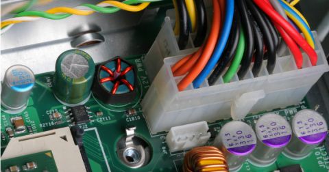
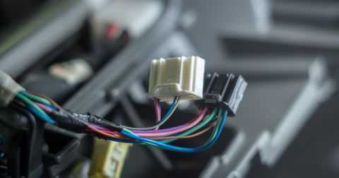
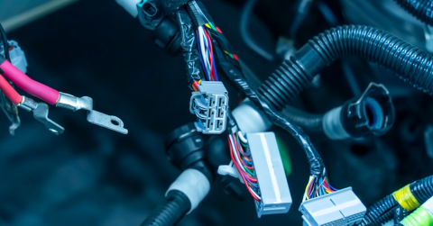
Wiring issues during design can lead to malfunctions, unreliable connections, expensive redesigns, and production delays. Electrical wire harnesses involve collections of wires, connectors, and terminals, all of which must correctly align with the PCB layout.
Without the right integration tools, mismatches between schematic and physical layout often occur. These inconsistencies result in flawed paths or unusable connections, jeopardizing the functionality of the final product.
How Altium Addresses Wiring Mistakes
Altium delivers a unified design solution tailored to prevent wiring errors in cable harness design. Its features enable faster validation, reduce redundant tasks, and support robust PCB-to-harness integration.
1. Complete Harness Design Integration
Altium offers a visual, intuitive environment for building custom wire harnesses directly alongside PCB layouts. The Harness Design feature allows teams to configure connectors, terminals, and wires inside the same workspace used for board development. This cohesive view ensures clean connections and avoids mismatched or incomplete designs.

2. Multiboard to Harness Integration
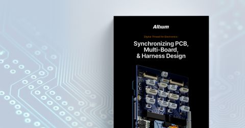
Spend more time creating complex designs and less time learning how to integrate multiple boards in your design tools. With the same design approach and editors used for single-board designs, Altium intuitively empowers designers of all levels to create interconnections between multiple boards. With harness design synchronization, you have everything you need to complete your multi-board projects. Keep changes automatically in sync when a harness project is created as part of a multiboard project. Design changes remain consistent between connectors and parent PCBs.

3. ECAD-MCAD Integration
Altium's MCAD codesign capabilities allow engineers to push the harness definition from ECAD to MCAD, where the mechanical engineer can define the cable routing through the enclosure and the connections to the printed circuit boards. The 3D harness definition can then be pushed back from MCAD to ECAD as part of the multi-board assembly. The physical length of wires, cables, and harness segments is assigned to the corresponding Harness entities in ECAD.

4. Harness-to-PCB Design Visualization
Visualizing the harness and PCB within one tool dramatically reduces the possibility of mistakes. Altium lets you preview how the harness would be physically connected with the PCB because the software supports 3D visualization. You then use this view to verify possible routing problems, incorrect connectors, or issues about clearance violations.

5. Better Collaboration Between Teams
Altium allows for real-time collaboration in complex designs where multiple teams may work on different aspects of the harness or a PCB. Design teams can easily share their work, comment on design elements, and make real-time updates. The benefit of this collaborative approach includes avoiding communication breakdowns that can lead to wiring errors and ensuring all team members are on the same page when it comes to harness-to-PCB integration.

Benefits of Using Altium Designer for Harness-to-PCB Integration
By applying Altium's advanced harness-to-PCB integration tools, you can expect several key benefits:
- Fewer Errors: Spot and fix errors during the design phase, not during production.
- Faster Time to Market: Integrated workflows and early error detection prevent costly delays.
- Better Accuracy in Design: Real-time validation confirms the harness and PCB align as intended.
- Improved Collaboration: Shared workspaces reduce confusion across design teams.
- Increased Efficiency in Design: Engineers spend less time troubleshooting and more time building.
Design with Confidence: Eliminating Wiring Errors at the Source
Harness-to-PCB integration doesn't have to be cumbersome and error-ridden. Altium has a complete set of tools engineers need to create seamless, accurate designs with fewer mistakes. From real-time error checking and advanced validation to enhanced collaboration, Altium gives you what you need to avoid wiring errors and ensure your design is ready for production.
Want to avoid wiring mistakes in your integration from harness to PCB? Experience the power of wire harness design in Altium Develop!


