


Avoid Costly Wiring Errors in PCB Projects with Integrated Harness Tool

At a Glance
Avoid costly PCB wiring errors with Altium integrated harness tool. Detect issues early, optimize routing, and improve collaboration.


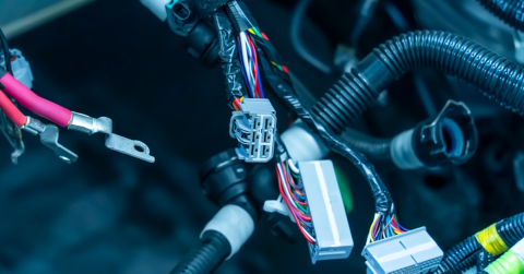
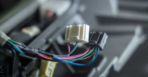
Wiring errors disrupt timelines, inflate costs, and complicate even the most well-planned PCB projects. Whether you engineer complex systems or prototype first-run designs, detecting these errors early prevents rework, miscommunication, and manufacturing delays.
If wiring mismatches and harness mismanagement still slip through your current workflow, Altium’s integrated harness tool offers a system-level solution. This feature consolidates PCB and wire harness development into a single, intelligent platform, empowering teams to detect and correct costly wiring errors before they derail progress.
What Is Altium's Integrated Harness Tool?
Altium integrates logical and physical wire harness design into one streamlined environment. Instead of toggling between disjointed tools or managing disconnected datasets, engineers access a unified workspace that synchronizes every connection, pin assignment, and cable route in real time.
This design environment supports:
-
Precise connector configuration and pin mapping
-
Consistent updates across schematic and layout views
-
System-wide visibility into how every harness integrates into the larger PCB
Whether you route wires through tight enclosures or define cable paths for automotive systems, Altium ensures your layout reflects both electrical logic and physical design realities.
How Altium Can Help Prevent Wiring Errors
1. Real-Time Error Detection and Resolution
Altium runs continuous Design Rule Checks (DRCs), flagging misrouted wires, improper pin assignments, and disconnected nodes as you work. These checks adapt to your project's specific constraints, enabling you to correct issues during design rather than after fabrication.
2. Enhanced Visualization Through 3D Design Context
Accurate harness design requires spatial awareness. Altium provides 3D design views that show how wires, connectors, and PCB components interact within the enclosure. Engineers can inspect fitment, verify clearances, and detect routing congestion before finalizing layouts.
3. Synchronized Team Collaboration
Designers, electrical engineers, and manufacturers access a centralized dataset within Altium, ensuring alignment across all disciplines. Changes propagate across all views and documentation, removing ambiguity and reducing the risk of implementing outdated revisions.
4. Adaptive Updates That Preserve Design Integrity
As projects evolve, your design may change. Altium makes updating and modifying your designs easy without introducing new errors. When a component or layout changes, Altium automatically updates the entire design—there is no need to manually update individual wiring diagrams or track down mismatches. This streamlined process ensures that your design stays current without the risk of introducing wiring errors along the way.
5. Optimized Routing and Wire Lengths for Enhanced Performance
Altium’s harness tools optimize wire lengths, routing paths, and connector orientation to ensure logical, efficient harness construction. The result: cleaner designs, improved assembly, and higher system performance with fewer chances for human error or signal degradation.
Real-World Use Case: Automotive PCB Integration
Consider a high-density automotive PCB system that requires coordinating multiple sensors, controllers, and actuators. Without an integrated harness platform, managing routing constraints, connector standards, and pin assignments across spreadsheets and siloed tools increases the risk of oversight.
Using Altium’s integrated harness tool, the design team manages the entire cable architecture alongside the PCB. Every modification updates instantly across schematics and harness documentation. Real-time error notifications, visual wire path validation, and multi-board assembly views allow the team to validate all constraints—mechanical, electrical, and functional—before prototyping.
This streamlined approach avoids costly miscommunication, reduces design cycle length, and guarantees compatibility between the harness and the PCB.
User Testimonials: What Engineers Are Saying About Altium’s Harness Tool
Here’s what engineers are saying about Altium’s harness design feature:
Creating harnesses, cables, and wired assemblies is much easier and faster, and it also produces nice documentation for manufacturing.
- Senior Electrical Engineer, Cryogenic Systems
All our designs are done in Altium, supporting all of that from the PCB design element all the way through cabling design, system design, and speccing off-the-shelf parts and systems.
- Senior Electrical Engineer, Agricultural Robotics
The Long-Term Benefits: Save Time, Save Money
While adopting Altium's harness design tool might require an initial commitment, the long-term savings and efficiency gains make it a wise choice. By preventing wiring errors early on, you save time that would otherwise be spent troubleshooting and fixing issues later in the process. You also avoid costly manufacturing delays or design revisions that might arise due to mistakes in the wiring phase.
Additionally, with Altium’s optimized routing and wire management, you may reduce material waste, shorten manufacturing time, and improve the efficiency of the assembly process. Ultimately, this leads to a more cost-effective production cycle and a more reliable final product.
The Key to Better, More Reliable PCB and Harness Designs
Wiring mistakes can derail even the best-engineered systems. Altium’s integrated harness environment resolves these issues before they compound, combining real-time error detection, 3D visualization, and collaborative version control into one powerful design workflow.
If your team aims to improve design quality, reduce manual rework, and build high-performance products without last-minute wiring surprises, it’s time to move beyond disconnected workflows.
So, if you want to take your PCB and harness designs to the next level and avoid the headaches of wiring errors, it’s time to explore what Altium’s harness design tool can do for you. Experience the power of wire harness design in Altium Develop.

About Author
Related Resources
Related Technical Documentation
Table of Contents
- What Is Altium's Integrated Harness Tool?
- How Altium Can Help Prevent Wiring Errors
- 1. Real-Time Error Detection and Resolution
- 2. Enhanced Visualization Through 3D Design Context
- 3. Synchronized Team Collaboration
- 4. Adaptive Updates That Preserve Design Integrity
- 5. Optimized Routing and Wire Lengths for Enhanced Performance
- Real-World Use Case: Automotive PCB Integration
- User Testimonials: What Engineers Are Saying About Altium’s Harness Tool
- The Long-Term Benefits: Save Time, Save Money
- The Key to Better, More Reliable PCB and Harness Designs
Design to Release, Without the Friction
- Keep reviews tied to the right version
- Reduce handoff confusion and rework
- Spot sourcing and release risk earlier
- Work solo, share when needed
Get Started
Thank you, you are now subscribed to updates.

