Backdrill-and-Fill For Blind and Buried Vias in PCBs
Blind vias aren’t just for HDI PCBs, they are also used in standard builds with mechanical drilling and no thin outer layers or build-up film layers. These designs find their home in many different systems, and for me this is most common in high-speed designs or RF designs that require terminated holes for press-fit pins or threaded pins. No matter what the application is, the presence of these holes drives a multiple lamination process to drill, plate, and press the layers into the PCB stackup.
The number of laminations required to build a PCB is a decent proxy for price assuming a traditional etching and mechanical drilling process. Depending on how blind/buried vias are used in a PCB, the number of laminations may not match your initial count. Therefore, before you start placing blind and buried vias in your PCB stackup, note that your fabricator might take an alternative approach to build your PCB, which could impact total costs and routing area. I’ll look at how placement of blind and buried vias impacts the number of lamination cycles and, ultimately, the number of processing steps and costs associated with the build.
The Cost of Lamination Cycles
Each lamination cycle in PCB fabrication brings a drilling and plating step, and this is how we are able to form blind/buried vias in a PCB stackup. When blind/buried vias are present in a design, multiple lamination steps are used to bond each group of etched layers to create the final stackup. Each lamination cycle adds processing steps and thus adds cost to the design. Although blind vias are absolutely necessary in many products, some simple considerations on the order of processing steps can offset some of the additional cost and help keep your product competitive.
Normally, we would just count up the number of layer spans requiring blind/buried vias, add 1 cycle for the central core or the capping layers on the outside of the stackup, and we get the total number of required laminations. For example, consider the stackup below with a through-hole via and buried via for embedded printed RF circuits, which I discuss in more detail in another article.
In this example, we have a symmetric stackup that requires two lamination cycles: one for the embedded buried via, and another cycle for the two outer layers. This is a simple example that illustrates the standard multi-lamination process required to form blind/buried vias.
There are instances where the use of blind/buried vias may allow fewer lamination cycles or a different processing approach than simply using sequential lamination like we might find in one of the standard HDI stackups. Some of these instances include:
- Blind vias starting from one surface layer or offset buried vias (non-hybrid builds)
- Stackups with crossing blind/buried vias
- Hybrid stackups with blind/buried vias
- Reverse stackups (or cap-core stackups)
Backdrill-and-Fill
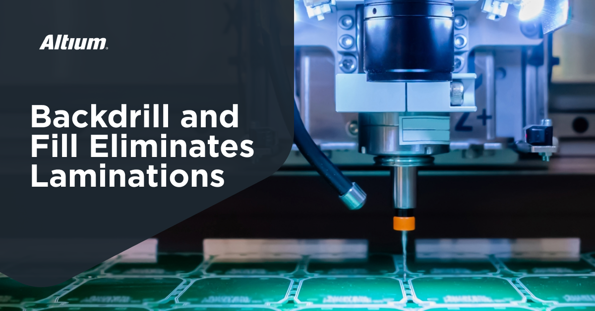
An alternative process that can be used instead of sequential lamination is to backdrill-and-fill in specific layers as this might eliminate one or more lamination steps. In backdrill-and-fill, a blind or buried via is formed past the layer span where it is needed, but then the fabricator backdrills the blind/buried via to length. This terminates the via on the desired layer, and the leftover space in the drilled dielectric is filled with non-conductive epoxy. The filled area may then be plated over, such as instances where the drilled layer is a copper plane layer.
In some of the examples given above, this may be a preferred way to fabricate some of the stackups as it could eliminate one or more lamination cycles. A bit of anticipation of the processing steps in these examples will help you better plan your use of blind/buried vias, and possibly eliminate some lamination steps in PCB fabrication.
Asymmetric Blind/Buried Vias
PCB fabrication generally assumes and proceeds with symmetricity in the layer arrangement, and thus in lamination. However, PCB stackups with blind/buried vias may not use symmetric placement in the stackup. For example, with a buried via such as the case below, this will be a classic case where backdrill-and-fill is evaluated as the fabrication solution instead of using an additional lamination.
In this example, keeping the layer stackup symmetric during fabrication would cause two possible processes:
- Fabricate L3-L6 first, followed by L2/L7 and L1/L8 layer pairs (3 laminations total)
- Fabricated L2-L7 first, backdrill-and-fill, and finish with L1/L8 layer pair (2 laminations total)
In the L6-L7 backdrill and fill process, the backdrill has a potential to break traces in the neighborhood of the drills. Obviously, this eliminates the main advantage of using blind/buried vias, which is to allow some routing space by keeping the via barrel and pads away from traces outside the layer span. Therefore, this works best if the backdrilled portion only involves drilling through copper pour or a plane layer. With a plane layer, the backdrill will cut through copper, but the required re-plating of copper will be the same everywhere and thus standard plating can be used to re-form the copper.
Crossing Blind/Buried Vias
Now let’s examine the case of blind/buried vias which are crossing each other in different layer spans, which would normally not be manufacturable in standard stack-drill-plate fabrication. This case is the interesting as it can also involve offset (asymmetric) arrangements of blind/buried vias, which then also cross each other in the PCB stackup. While there are some electrical reasons you might need these crossing blind/buried vias, creative layer assignments could allow for a backdrill-and-fill process on some layer spans.
For example, consider the following stackup. This may involve multiple blind vias crossing each other in the stackup, leading to multiple rounds of backdrill-and-fill during fabrication.
In a backdrill-and-fill fabrication process for this stackup, the typical view would be that the design takes two sub-laminations with drill and plating, followed by drilling and plating the through-hole vias. However, the mixed larger via and buried via might actually proceed as follows:
- One of the blind/buried sections (either L3 to L8 ot L1 to L6) is fabricated first with complete through-hole drilling and plating down through the entire blind-buried layer span (L1 to L9)
- During the next lamination cycle, the newer via is placed as a through-hole and then back-drilled and filled; the copper on the outer-most portion of this lamination can be recovered during cap plating
- The final L1-L10 through-holes are drilled and plated to complete the stackup
There could be reasons that a dedicated blind via with a specific layer span is needed, even if its span crosses over a different layer span. One use case I mentioned above is the embedded RF circuits case, another is the press-fit pins case with a thick PCB stackup. Another use case is to eliminate a backdrill on a pin insertion for a high-speed connector transition. Whatever the use case may be, every crossing blind/buried via will create more costs, so focus on which crossovers you can consolidate and floorplan important signals around these transitions.
Hybrid Stackups With Blind Vias
Hybrid stackups are designs where the PCB stackup uses a mixture of material sets. Most commonly this involves the use of PTFE and standard FR4 materials for RF+digital designs (which I have talked about extensively in other articles), but of course other material sets can be mixed as well. When these stackups include blind/buried vias, they will also require multiple laminations as one would expect.
The question with a hybrid stackup is whether to laminate the individual hybrid laminations first and stackup/plate these to form through-holes, or whether to put each hybrid layer on individually and drill/plate it to form the final vias. For example, take a look at the material grouping for a hybrid stackup shown below.
From this, we can see two potential areas where backdrill-and-fill might be applied:
- From L1 to L2 on the 2:3 buried via
- From L5 to L6 on the 6:10 blind via
On the outer hybrid material set, it does not make much sense to perform backdrill-and-fill to form the outer small buried via. For the inner vias, it might make more sense given that the overlapping blind vias only miss each other by one layer. In this case, as long as the backdrilled layer span involves a plane layer or it cleared and has no traces, backdrill-and-fill would eliminate one of the laminations.
Reverse Stackup (a.k.a. Cap-Core Stackups)
Cap-core stackups effectively place planes on the outer layers and use buried vias on the inner signal layers to route signal traces. Through-holes are used to reach components on the other layers and to stitch the external planes together. The simplest example is with a 4-layer PCB, where the two internal layers are used for signal and are routed with buried vias. With higher layer count, The outer cap layers will still require the final laminations prior to through-hole drilling and plating, but the inner layers could use a backdrill-and-fill process instead of a sequential lamination. This is shown in the cap-core stackup below.
There are two regions where backdrill-and-fill would be required to fabricate this. Either the shorter vias or the longer vias would need to be backdrilled; in this case it makes most sense to form a sub-lamination from L2 to L9, and then backdrill-and-fill the larger buried vias. The cap layer is then applied to form the final cap-core stackup.
Summary
Whenever plating is used after backdrilling, there could be a dimple on the plating area in the re-plated layer. This dimple will normally be as small as ~1 mil. When backdrill-and-fill is applied, it is normally on mechanically drilled blind/buried vias, which will occupy thicker dielectrics. Therefore, in most practical cases, the leftover dimple will not impact the natural thickness variation of the dielectric layer.
While it might seem paradoxical to bring backdrilling into a PCB via design that is intended to eliminate backdrilling, it illustrates that judicious and targeted use of backdrilling ends up being a big cost saver and allows fabrication of some stackups that would normally not be manufacturable. It illustrates that PCB stackup engineering involves many tradeoffs relating to cost, performance, and manufacturability.
Whether you need to build reliable power electronics or advanced digital systems, use the complete set of PCB design features and world-class CAD tools in Altium Designer®. To implement collaboration in today’s cross-disciplinary environment, innovative companies are using the Altium 365™ platform to easily share design data and put projects into manufacturing.
We have only scratched the surface of what’s possible with Altium Designer on Altium 365. Start your free trial of Altium Designer + Altium 365 today.

