The Best PCB Antenna Design Software Eases Antenna Implementation

Circuit Board antenna design can be a difficult task for any software; however, that shouldn’t be a problem for Altium Designer, which can serve as your go-to BLE antenna design software and much more.
ALTIUM DESIGNER
Ensuring that your antenna designs are placed without issue
Consumer and industrial demand have prompted the demand for smaller wireless devices. The devices support wearable technologies, Bluetooth Low Energy (BLE) applications, personal communication systems, Internet of Things (IoT) applications, medical technologies, automotive advanced driver-assistance systems, and other innovative technologies. Each of these and other applications requires PCB antennas that reduce the physical footprint and cost while maintaining performance. In addition, PCB antenna designs must also respond to frequency requirements that range from the typical 2.4 GHz band to millimeter-wave frequencies.
Instead of using a three-dimensional wire that extends over the PCB or a chip antenna, a PCB antenna design software consists of a trace drawn on a Printed Circuit Board. Depending on the type of antenna and the space constraints, the type of traces used for PCB antenna designer includes straight traces, inverted F-type traces, meandered traces, circular traces, or curved trace that has wiggles. The two-dimensional structure of the PCB antenna requires robust antenna design software such as Altium Designer to ensure that the structure meets the specifications given by the manufacturer.
The Best PCB Antenna Simulation Software Matches Innovation to Application
Manufacturers may offer PCB antennas as already fabricated components that include cables and connectors. With the array of available PCB antenna options (e.g. BLE antenna design, IoT antenna, etc.), a team can add to the system design or customize an antenna according to electrical and mechanical requirements. PCB antenna designs range from basic microstrip patches to combinations of microstrip patches, strip lines, and coplanar waveguide (CPW) transmission lines. Some designs may combine different types of transmission lines within the same PCB antenna.
Choosing a PCB antenna design software depends on the application. A wireless mouse does not need the same RF range and data rate that other applications may require. Sensors and devices connected to the Internet of Things require larger RF ranges and higher data rates. Newer PCB antenna designs feature dual-band and multiple-frequency band coverage as a response to system applications that require wideband frequency ranges or multiple applications served by the same antenna.
Because of the variation in RF ranges, designs that have the same power requirements often have different layouts and apply different principles for antenna design. Regardless of the application, the design of the antenna and the RF layout has the greatest impact on performance. In addition, a PCB antenna simulation software must follow layout guidelines for the RF traces, adhere to best practices in PCB stack-up and grounding, provide power supply decoupling, and be comprised of the proper RF passive components. Differences in design and product requirements establish the need for PCB antenna design software.
As an example, some high-frequency applications that do not require higher gain use monopole PCB antennas that consist of a microstrip patch formed on one side of a circuit laminate separated from a larger ground plane by a dielectric. Other applications may require higher gain at certain frequencies and use multi-layer configurations. In either instance, the wavelength of the target operating frequency has a direct relationship with the size of the patch.
PCB Antenna Design Requires a Fundamental Approach
PCB antenna design begins with establishing key performance parameters. Those parameters include
- Return loss
- Bandwidth
- Radiation efficiency
- Radiation pattern, and
- Gain.
Every antenna must match with a signal feed that has a typical characteristic impedance of 50 ohms. The return loss of an antenna indicates the quality of the matching by showing the quantity of incident power (dB) reflected by the antenna because of a mismatch. An infinite return loss shows that the antenna matches the signal feed. Perfect antenna designs radiate all energy without any reflection. Generally, design teams find a return loss of 10 dB as sufficient; 90 % of the incident power goes to the antenna for radiation.
The bandwidth of an antenna measures the frequency response of the antenna. To place this in a different perspective, the bandwidth measures the ability of the antenna to match the signal feed over the entire band of interest. When considering BLE antenna design, the greatest losses occur at 2.33 GHz and 2.55 GHz while the lowest losses and best efficiency occur between 2.40 GHz and 2.48 GHz. Most consumer devices use a wider bandwidth to minimize the effect of detuning caused by the operating environment.
Radiation efficiency describes the amount of non-reflected power dissipated as heat or thermal loss in an antenna. 100 percent radiation efficiency shows that all non-reflected power radiates into free space. In PCB antenna designs, thermal loss occurs through the dielectric loss in the FR4 substrate and conductor loss in the traces. Small form-factor PCB antennas have the lowest thermal loss and the highest radiation efficiency.
Along with radiation efficiency, antennas have a specific radiation power. Ideal antenna behavior radiates power equally in all directions in the plane perpendicular to the antenna axis. Most PCB antennas have excellent--but less than ideal--radiation efficiency with omnidirectional patterns. Because the radiation pattern shows the directions that have the highest and lowest radiation, the radiation efficiency shows how to orient the antenna for the application. The gain (dBi) of an antenna measures the strength of radiation in the direction of interest when compared to the ideal behavior.
Along with observing those parameters, PCB antennas require the proper size ground plane for optimal performance. From a simple design perspective, the antenna behaves as an LC resonator. The resonant frequency decreases with increases in either inductance or capacitance. Larger ground planes increase capacitance and decrease the resonant frequency. Better grounding also achieves better return loss. Establishing the correct ground allows the PCB antenna designer to have better performance.
- Read about ceramic chip antennas versus PCB trace antennas
- Learn about BLE antenna design for your PCB
- Read how to use GPS antennas in your design
PCB Antenna Design Presents Challenges
Several different challenges confront teams seeking to design high-performance PCB antennas. Some applications may use multiple antennas at both the transmitter and the receiver sides to improve the performance of an antenna system. However, antenna elements that have close proximity to one another may begin to interact with mutual coupling. Each reaction between elements affects the ability of the array to maintain good impedance matching and wastes power. In addition, the electromagnetic coupling disturbs the radiation pattern of the antenna, inhibits gain, and affects the resonant frequency.
Another challenge involves the effect of the enclosure on antenna sensitivity. Many times, the plastic used for an enclosure will have a higher dielectric constant than air. The lack of sufficient clearance between the antenna and the enclosure causes the antenna to see a higher effective dielectric constant. As a result, the electrical length of the antenna increases and the resonant frequency decreases. Design teams should always verify the performance of the antenna matching network with the final plastic enclosure in place and the product installed in a typical use scenario.
At high frequencies, the impedance of an RF circuit changes when measured at different distances from the load. The width and thickness of the RF trace, the clearance between the trace and ground along with the substrate type also affect the amount of impedance change. In a PCB antenna design, coaxial cables, microstrip lines, and coplanar waveguides function as transmission lines. Common practices involve using a passive circuit as a matching network to transform the characteristic impedance of the RF trace and to ensure the maximum power transfer between the matching source and load impedances.
The use of high-speed circuits within electronic products that utilize PCB antennas increases the risk of electromagnetic interference and radiated emissions. Simultaneous Switching Noise (SSN) caused by the downscaling of integrated circuits and the increased clock frequencies of microprocessors results in self-jamming—or the introduction of signals that negatively affect the signal-to-noise ratio and distort the signal transmitted by an antenna. In the same way, the antenna can cause self-jamming along its transmission lines and degrade signals throughout the PCB.
What Does Good Antenna Design Software Provide?
PCB antenna design software accurately analyzes the filters, microstrip lines, and passive components that make up a PCB antenna. The software also assists with PCB antenna design by displaying metal-dielectric layers, feeds, and connector types. To meet modern design requirements, PCB antenna simulation software provides the antenna's geometrical and electrical properties for optimal performance. Establishing these properties allows the software to model the correct antenna impedance and radiation pattern.
- Utilize design principles for an inverted-F antenna in your PCB design
- Keep EMI in check with a dual-band antenna design
- Learn about using hybrid or compact fractal antennas

Analysis and simulation are only parts of the design process
Altium Designer Solves Circuit Board Antenna Challenges
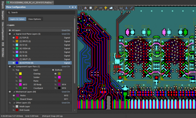
Altium Designer provides the Schematic Editor, the PCB Editor, and signal integrity analysis tools for controlling and matching impedances needed for consistent PCB antenna performance. The Schematic Editor and PCB Editor ensure that impedance matching occurs from the output pin to the target input pin. In addition, the Editors suggest the addition of termination components to achieve matching throughout the circuit and decoupling capacitors or materials used to prevent the mutual coupling between PCB antennas. Teams can find the correct components for supporting something like a BLE antenna design through database libraries or the Altium Vault.
Signal Integrity Analysis tools in Altium Designer identify any nets that could have unacceptable levels of reflection. The tools also predict potential levels of signal reflection and crosstalk while providing a what-if analysis of potential termination components. The combination of the Editors, Design Rules, and Active Route ensures that the correct routing path for the signal occurs and that an unbroken path for the return current exists under the signal route. With these techniques, Altium Designer prevents EMI and provides the best design for optimal PCB antenna design performance.
While placing shields on clocks, microcontrollers, and switching power supplies provides one solution for eliminating EMI, any shielding will block transmitted signals and should not cover the PCB antenna design. Altium Designer can protect against self-jamming with a combination of design rules for routing and its Active Route function. The output traces from the clock should run over the ground plane to reduce any current induced by stray RF fields and minimize loop areas. Altium Designer also assists with eliminating net PCB antennas that can cause self-jamming through the optimal placement of ground planes. Any ground plane placed directly below the clock allows forms a net antenna.
Altium’s Layer Stack Manager defines the layers used in a Printed Circuit Board design and governs the types of layers included in the stack. When designing a PCB antenna, teams can use the Layer Stack Manager to specify each layer for the type of material, the thickness, and the dielectric constant. Altium Designer also includes the Characteristic Impedance Driven Width option in the Routing Width design rule. The option applies an industry-standard equation to translate the impedance into a width setting.
Altium Designer also provides 3D PCB layout tools that allow teams to see the impact of mechanical data on the PCB antenna. Design teams can import the component model into the library editor and the enclosure into the PCB Editor to perform accurate collision testing. Because Altium Designer enables ECAD and MCAD collaboration, the software allows teams to work with external physical constraints and select the appropriate board shape. With these tools, design teams make the needed adjustments for circuits and enclosures to ensure that the plastic does not affect the dielectric constant.
Altium’s Unified Design Environment Makes PCB Antenna Design Easier
While many PCB antenna simulation software applications provide needed tools, Altium Designer places schematic and Circuit Board tools in one environment. Powerful design tools such as the Layer Stack Manager and Signal Integrity Analysis tools respond to the same menus, commands, and function keys. The complete suite of tools found within Altium’s unified design environment moves concepts from schematic to PCB layout to design documentation and to fabrication and production.
- Learn about layer stack definitions for your circuit boards in Altium Designer.
- Learn about Altium Designer's interactive routing.
- Learn about Altium Designer's smart component placement.

Be secure in your designs, no matter what they are.
Altium Designer’s innovative software is capable of achieving and succeeding in any of your potential design needs, including BLE antenna design, medical devices, IoT designs, etc. Give your circuit boards the security to be transferred through to production in the most accurate and stable way. Trust Altium Designer to get your electronics done right.


