Embedded RF Design: Ceramic Chip Antennas vs. PCB Trace Antennas

Over the years, there’s been a large rise in café culture which has left many of the newer cafés looking for ways of adding a creative interest to their store. Café and bookstore hybrids, gourmet coffee with baristas that have an expertise over regional coffee beans, and even cat cafés have all been twists I’ve seen pop-up.
When it comes down to it, people are going to cafés for a few key reasons though: to get a drink or snack, to meet and talk with their friends, or to get some work done outside of their office and house. The cherry-on-top may be what differentiates the stores, but the core concepts are relatively unchanged. This is very similar to choosing between component options for PCB antenna performance.
The demand for a compact, high performance, and low-cost embedded RF transceiver solution has been on the rise with developments in robotics, AI, and IoT for many years. It remains that cost, board layout, DDR3 layout guidelines, and expertise are the key characteristics that influence the designer's preference on a ceramic antenna vs PCB antenna design.
PCB Antennas: Know Your Frequency Range
In the past, the design engineer may consider the tradeoffs for their target frequency range and op for the more reliable trace antenna. Modern embedded antenna hardware is designated to operate in a bandwidth sandwiched somewhere between 400 megahertz and 5.5 gigahertz. With ceramic antenna implementation becoming increasingly reliable, affordable, and straightforward perhaps the competition is beginning to sizzle.
The fact is that the outlay of a simple wire trace on a PCB ground plane that is placed down by the in CAD, before fabrication, is minimal. Despite the low-cost nature of the trace antenna, there are yet still many instances where the ceramic chip antenna is preferred. The cost can be offset by the small size, greater ease of implementation, and higher tolerance to environmental interferences that the ceramic chip antenna offers.
PCB Trace Antennas
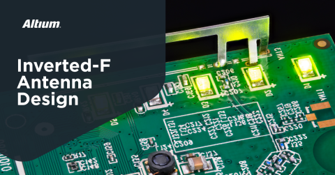
Printed circuit board trace antennas are notoriously difficult to design, implement, and tune; particularly in a small and reliable implementation. Similar to a wire antenna, a trace antenna's size will depend on the frequencies of the target bandwidth. For example, at low frequencies, the length of the trace antenna will have to be much longer for the signal integrity to resonance frequency.
The advantages in choosing a PCB trace antenna over a ceramic chip antenna are:
- The trace antenna is embedded into the PCB board during the manufacturing process.
- When optimally tuned, a trace antenna can operate within a wide bandwidth while commanding a high level of network reliability and strength.
- Trace Antennas have a thin profile.
The disadvantages of using printed circuit board trace antennas can be:
- Difficulty to design, particularly at low frequencies. They are highly susceptible to changes to the board layout requiring tuning after each change, if not remanufacturing.
- They take up much more space than a ceramic chip antenna, particularly true if designing for low frequencies. The larger PCB area that is occupied will increase the cost of the design.
- Trace antennas are highly susceptible to environmental interferences.
The PCB trace antenna cannot be physically modified by the after manufacturing. If changes are required, the user will have to modify the antenna design and manufacture the board again. The potentially large size of the PCB antenna and time-consuming nature of the design/tuning process which generally involves utilizing PCB simulation software and extensive testing can be motivational factors for the board to substitute a ceramic chip antenna instead.
Ceramic Chip Antennas
Ceramic chip antennas will generally also require tuning by a network design, but they lack the physical properties of the trace antenna that cannot be manipulated after the board is printed. This eliminates the need for simulation software and costly manufacturing of new prototype boards in which case the prior components would go to waste.
Ceramic chip antennas can offer several advantages of their own:
- Small size and an assortment of configurations are obtainable.
- They are not as sensitive to the proximity interference of environmental noise and components.
- Changes to the board design guidelines or ddr layout are more easily accommodated without a need for simulation. The ceramic chip antenna can be more readily tuned or even replaced.
- Ceramic chip antennas have their disadvantages as well:
- There is a higher initial cost when purchasing ceramic chip antennas and their required support components. Currently, the average chip antenna will cost between $0.10 and $1.60.
The ceramic chip antenna is a component that you add to the board after the design phase has been completed. This feature allows for greater tuning versatility during development. The surface mount feature of the ceramic chip antennas allows for them to be easily removed and replaced to accommodate quick hardware modifications.
Creating an antenna design with ceramic chip antennas allows for more open board space to incorporate additional desirable components. This extra freedom could also be forfeited for a reduced board size to save on manufacturing expenses. It would be critical for a high volume multi-layered PCB board design engineer to consider the real estate being wasted as each layer is added to a board schematic containing a PCB trace antenna.
It is a struggle to create the smallest possible size antenna while minimizing the tuning time and maximizing signal integrity strength but leaving room for another desirable matching component to be added. Regardless of the implementation method, it is best to extensively test the final prototype to determine over the air measurements that can be scrutinized for viability.
If tuning is necessary, it can be achieved much more quickly and easily with strong PCB design software. If you’re looking for software with great features such as auto interactive routing, a power distribution network design, and easy 2D-to-3D layout switching, Altium Designer® may have the unified design environment that you need to get your designing done right.
To further talk about what type of antennas are the best choice for your PCB guidelines, or to learn more about frequency needs in general, try talking to an expert at Altium Designer today.
