




Beyond the PCB Design Review - Mechanical, Thermal, and Code

At a Glance
Catch costly hardware failures early. Learn how multidisciplinary PCB design review integrates mechanical, thermal, and firmware validation before the first prototype.


While standard schematic and layout reviews ensure electrical viability, true hardware success demands validation far beyond the PCB designer’s traditional purview. A board with flawless signal integrity is useless if it violates enclosure z-axis heights, cooks its own components, or ships with swapped pins.
To prevent these late-stage failures, multidisciplinary engineering teams must abandon sequential handoffs and integrate mechanical, thermal, and firmware constraints into the earliest stages of the design review.
Altium Agile Teams gives multidisciplinary electronics teams the structured collaboration, shared visibility, and cross-discipline workflows they need to bring mechanical, thermal, and firmware stakeholders into the live design state without slowing the team down.
Key Takeaways
- Learn the pros of ECAD-MCAD synchronization. Mechanical engineers (MEs) provide critical spatial context to PCB designers, but they must be able to interact with live board data natively to prevent physical interference.
- Validate thermal dissipation pre-routing. To prevent localized hotspots, thermal engineers must analyze live 3D board data and component power profiles before the electrical engineer (EE) commits to final copper routing.
- Pre-approve the digital pinout. Firmware teams must analyze live schematic component placement and pin multiplexing to confidently build the Hardware Abstraction Layer (HAL) before the physical board is ever manufactured.
The Friction of Traditional Handoffs
Halting a layout to conduct a manual cross-domain handover destroys development timelines. Historically, hardware design relied on a siloed, waterfall process: the EE finishes the layout, exports static PDFs, CSV spreadsheets, and a STEP model of the PCB, and throws them over the wall to the next department. This disconnected workflow guarantees version control fragmentation, miscommunication, and Engineering Change Order (ECO) bloat.
A shift left approach fundamentally changes this paradigm. It moves testing, verification, and cross-team collaboration into the active design phase to catch fatal flaws before they necessitate expensive board respins.
While a comprehensive PCB review checklist is foundational, executing it through disconnected tools is where teams hemorrhage time and budget. Instead of exporting outdated files, stakeholders must view the design natively. Altium Agile Teams eliminates early-stage friction by aligning multidisciplinary experts around a single source of truth, allowing them to log constraints and verify outcomes in real time.
To understand how this preserves project momentum, we must look beyond the schematic at the three most critical integration boundaries: mechanical fit, thermal management, and firmware readiness.
Mechanical Integration: ECAD-MCAD Collaboration
The traditional divide between EEs and MEs frequently results in late-stage mechanical interference. Z-height violations, misaligned mounting holes, clashing enclosures, and connector mating failures are classic faults that only surface when the first physical prototype is assembled.
While isolated component mismatches will occasionally happen, recurring fitment errors are a symptom of a broken workflow, not poor engineering.
Solutions for Flawless Electromechanical Fit
- Contextual 3D Constraint Review: MEs must be able to pull live schematic data and physical board outlines directly into their native MCAD environment to design the product enclosure and user interface while accounting for mechanical tolerances.
- Interactive Spatial Validation: By utilizing real-time collision detection and live 3D clearance checking, teams can validate component choices early. This is especially critical when mapping complex rigid-flex folding paths.
- The Benefit: Validating interactively eliminates historical mismatch errors, particularly when dealing with unpredictable off-the-shelf components. Engineers immediately see the physical impact of their electrical decisions, preventing costly mechanical respins.
Thermal Considerations
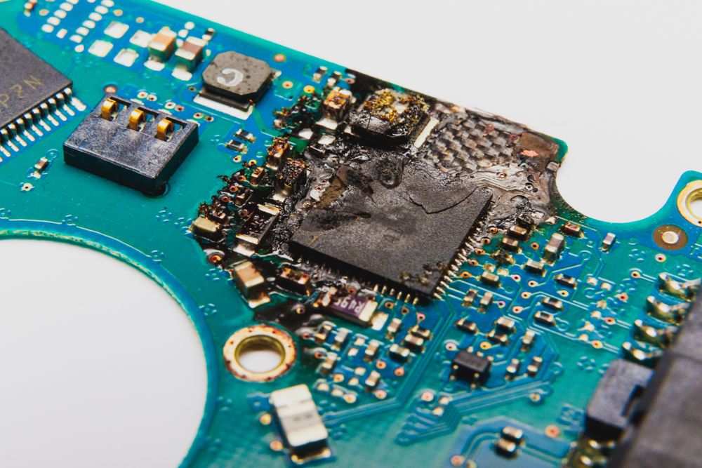
It is possible to develop an estimate of board temperature based on realistic component power dissipation, package thermal models, board stackup, copper distribution, and airflow assumptions. This should be part of the final verification process before releasing a design, not prior to routing or completing placement. While full qualification does not happen in ECAD software directly, it is possible to port a design into MCAD software via the cloud.
Within the Altium ecosystem, a PCB layout can be transferred directly to SOLIDWORKS or Ansys for thermal/CFD simulation. The ME verifies the imported geometry and assigns power dissipation, material properties, and boundary conditions in the external simulation environment. These inputs determine whether the proposed cooling arrangement maintains acceptable component temperatures.
The MCAD user can adjust enclosure geometry, fan selection and placement, and heatsink design and location. The results establish ECAD constraints such as heatsink clearances, thermal via requirements, and even the need for additional plane layers. Bringing this into the final verification loop allows heat management solutions to be identified before prototyping.

Firmware Readiness: Hardware and Software Co-Design
Many modern hardware products require firmware, and embedded engineers are often deeply involved in the PCB design review. Coding experts need early access to schematics to flag hardware decisions that conflict with the embedded firmware/software architecture.
Some of the classic firmware show-stoppers include swapped RX/TX pins, missing access to JTAG/SWD debug pins, or assigning pins to incompatible signals or interfaces. For large digital processors, firmware developers still rely on exported pinout spreadsheets, which become obsolete the exact second the EE saves a new schematic revision.
Solutions for Hardware-Software Co-Design
- Pre-Approved Digital Pinouts: Give firmware engineers access to the native schematic review. This allows them to verify pin assignments, validate bootstrap resistors, and confirm default pull-up/pull-down states prior to manufacturing.
- Continuous Schematic Visibility: Firmware teams can use a unified, cloud-based platform to view the live state of the schematic, allowing them to confidently utilize pin assignments and features without waiting for a final hardware freeze.
- The Benefit: Firmware re-writes (or equivalent hardware changes) can be identified early or avoided completely. When the first physical prototype arrives on the bench, the code is actually ready to run, eliminating the frustrating weeks of "bring-up" delays caused by simple pin-swap errors.
Step Away from Traditional PCB Design Review Routines
Manual handoffs create ambiguity and costly version mismatches.
Altium Agile Teams addresses this directly by giving multidisciplinary electronics teams the structure, shared visibility, and connected workflows they need to move from layout to review to release with greater consistency and confidence. Mechanical, thermal, and firmware contributors work from the same live design state, not exported snapshots, so the team catches conflicts early, reduces rework, and reaches manufacturing with fewer surprises.
By replacing siloed, sequential reviews with a concurrent, structured workflow, teams eliminate the ambiguity that causes late-stage failures. The result is projects that move forward faster, with fewer workarounds and significantly less rework.
Learn more about Altium Agile Teams →
Frequently Asked Questions
What is the goal of a PCB design review?
A PCB design review identifies errors in the schematic, layout, and manufacturing files before the physical board enters the prototype phase. It ensures the design is functional, manufacturable (as per DfM), and reliable in its intended application.
What is shift left in PCB design?
Shift left refers to moving testing, verification, and cross-team collaboration into the earliest stages of the design cycle. Instead of waiting for a finished board to identify functional errors, multi-disciplinary teams (mechanical, thermal, and firmware engineers) review the design while it is still fluid. This mitigates expensive reworks and prevents delays to projects.

About Author
Related Resources
Related Technical Documentation
Table of Contents
Speed at Scale. Structured Repeatability. Secure Flexibility.
- Start up fast with out‑of‑the‑box workflows
- Collaborate using ECAD‑MCAD codesign tools
- Manage BOMs with live supply chain part data
- Manage access and security as teams scale
Contact Us
Thank you, you are now subscribed to updates.