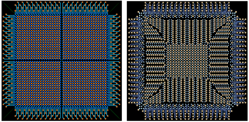
BGA Fanout Routing

How many times have you attempted to route into a BGA, only to be prevented by clearance and track width constraints? This is a time-consuming process in most design software, but Altium Designer has the tools you need to make this process easy. Rather than spending time manually modifying track widths in your BGA routing strategy, Altium Designer allows you to implement neck-down as you route into your BGA. You’ll also have a complete set of design tools for PCB design, including HDI design with fine-pitch BGAs.
ALTIUM DESIGNER
A fully-integrated PCB design suite that guides you from design to fabrication.
Due to the tight space under a BGA, using neck-down simplification for BGA routing becomes an important way to route impedance controlled traces into and out of a fine-pitch BGA. These traces might be quite wide to maintain desired impedance, and they might not fit between BGA balls on the surface or inner layers. Changing the width of the track as you route it is time consuming with most PCB design programs, but not with Altium Designer.
To alleviate this problem, using neck-down simplification for BGA routing is the answer. Neck-down is the process of shrinking the track width to a smaller width within rule constraints to allow for routing in tight spaces. With the full set of routing and layout features in Altium Designer, you can easily perform neck-down and create your escape routing strategy.
What is Neck-Down in BGA Fanout Routing?
PCB designers have become used to shrinking board sizes, pad sizes, via sizes, and component sizes. In addition, components with high I/O count come packaged in smaller footprints with finer pad pitch, making routing very difficult without the right design tools. In order to access the inner pads on a fine-pitch BGA, you need to shrink down the track width as it’s routed into the BGA pads. This process is called neck-down.
Typically, neck-down is defined the percentage width change between a pad size and track width. However, it is also possible to set a size reduction from track-to-track as it enters or leaves an area. The image below shows the primary challenge where applying copper neck-down during BGA fanout routing is useful. This controlled impedance trace needs to have specific width outside the BGA, so its width must be reduced to allow internal routing to the BGA pads.

Using copper neck-down as part of BGA fanout routing will help this trace reach an interior pad in a BGA.
Automate Fanout Routing in Altium Designer
All boards that you create in your PCB design software come with a set of design rules. One of those rules defines the track width of your routes. This rule, along with a clearance constraint rule, normally restricts the track from entering a BGA. Instead of manually changing your routing settings each time you need to enter/exit a BGA, the design rules in Altium Designer allow you to create sets of rules for different portions of your design. The single-ended and differential pair width rules for the design can be configured for a specific copper neck-down, saving you time when routing a dense BGA.
- Just like other components, BGAs come in a variety of packages. Each of these can have a different pad pitch, which requires changing your track width using neck-down.
- When your BGA becomes very dense, you’ll be forced into the HDI regime during BGA fanout routing and neck-down.
Learn more about designing your HDI stackup for fine-pitch BGAs.
- Some simple design steps can help you prevent signal integrity problems when creating your BGA fanout routing strategy and applying neck-down for differential pairs.
Learn more about signal integrity in BGA fanout routing and neck-down.

BGA routing on an exterior row and dog bone fanout for an interior set of BGA pads.
Choosing a BGA Fanout Routing Strategy
Because of the density and distance of BGA pads in fine-pitch components, only the two outermost rows of a BGA can be directly connected to copper traces on the surface. All other terminals of the BGA cannot be connected using a direct path. Fanout and escape routing often need to be used alongside neck-down routing to reach the internal pads in a BGA. Fanout and escape routing takes the interior and applies a specific routing pattern with a small trace at a 45 degree angle. This then connects to a blind via that forms a direct connection to the next signal layer. A single-ended trace or differential pair can then be routed to interior vias through an interior signal layer.
Automate Fanout Routing in Altium Designer
Altium Designer includes fanout routing strategies that are preprogrammed for BGAs, which helps save you time when routing a component with high pin count. You can set the fanout direction from the printed circuit board BGA pad and whether the a should be placed between terminals in the BGA (via placement mode).
In addition to standard fanout strategies, Altium Designer lets you place in-pads to eliminate the need for an additional trace between solder pads on the BGA. These vias can be microvias when you’re working with fine-pitch BGAs, allowing you to quickly reach the inner layers of your PCB.
- There are many fanout strategies for your BGA, and you can quickly implement any of these with the design and layout features in Altium Designer.
- BGA fanout is much easier when you use rules-driven design software to set your fanout parameters. Altium Designer makes this easy thanks to its rules-driven routing and layout features.
Learn more about using your design rules to help fanout a large BGA.
- The via design features are adaptable to BGA packages, allowing you to automatically place in-pad microvias for your fanout strategy.

Automatically create pin assignments and fanout patterns for your BGA escape routing.
Use Neck-Down Routing for Your BGA in Altium Designer
Once you’ve set up your design rules and room placement, neck down will be automatically applied to your traces as you route enter and exit the BGA. Altium Designer automatically changes the track size based on the rules for that room, and you can define new rooms for different BGAs in your PCB. Because Altium Designer operates in a rules-driven design environment, this process of automatically modifying track widths to fit in tight spaces is extremely easy.
Layout and Routing Are Easy in Altium Designer
The unified design environment in Altium Designer makes layout and routing extremely easy with a set of automated and semi-automated design tools. These features help you quickly layout powerful boards and route them easily, including into/out of BGAs with fine pitch. The online design rule checking tools will verify your layout as it’s created, giving you a complete set of design features for fine-pitch BGAs and much more.
- Powerful CAD tools are the cornerstone of Altium Designer. You’ll have a complete toolset for PCB design, layout, and manufacturing when you use Altium Designer.
- You can take control over your BGA fanout strategy and track layout with powerful routing tools in Altium Designer.
Learn more about the complete set of routing features in Altium Designer.
- ECAD/MCAD co-design tools in your PCB design software let you verify and route your design in 3D. You’ll have a complete solution for electronics design.

You can view and route your BGA fanout in 3D in Altium Designer
BGA fanout routing is easy with the complete set of PCB layout and routing features in Altium Designer. When you’re looking for a circuit board design program to make high density routing easy, use the complete set of PCB design features in Altium Designer.
Altium Designer on Altium 365 delivers an unprecedented amount of integration to the electronics industry until now relegated to the world of software development, allowing designers to work from home and reach unprecedented levels of efficiency.
We have only scratched the surface of what is possible to do with Altium Designer on Altium 365. You can check the product page for a more in-depth feature description or one of the On-Demand Webinars.


