


Microvia Technology and Beyond for HDI Design


HDI PCBs, ultra-HDI, packaging, substrate-like PCBs, and highly advanced chip-on-board can all require microvia structures once electrical connections become very dense. In these designs, higher density chipsets and packages have driven the demand for more advanced fabrication capacity that can support microvias into advanced stackups. But in addition to microvias in standardized HDI stack ups, there are more advanced interconnects available for routing.
Of the vertical interconnect architectures that exist, the more advanced versions of these are combinations of other interconnects, or totally new structures for vertical transitions in HDI PCBs. These structures work with laser drilling and stackup construction via sequential buildup (SBU).
Groups of microvias in standardized HDI stack ups and the non-standard HDs backups, as well as more advanced vertical interconnects, can still be built with the sequential buildup process. More advanced stackups require multiple lamination steps and close collaboration with the manufacturer regarding the allowed via transitions. With that in mind, follow us on a journey as we look at all the available vertical routing transitions in HDI PCBs.
Types of Microvias in HDI PCBs
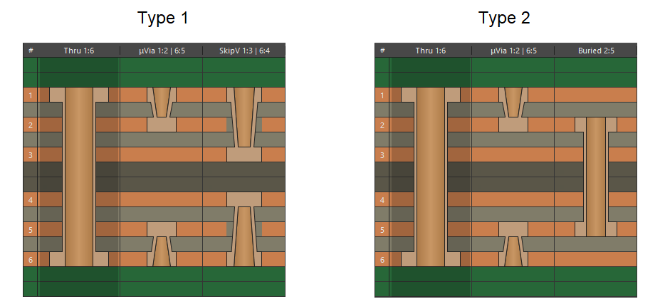
The various types of microvias used in HDI PCBs were developed to support standardized buildups. For example, take a look at 2+N+2 HDI (Type 2) stackups, which use blind and buried vias. Other standardized HDs stackups use different types of vias.
Blind and buried arrangements are the standard tools used in HDI stack-ups, particularly in sequential buildup around a central core. This is the case in both Type 1 and Type 2 HDI PCB stackups, as well as in non-standard HDI stackups. In Type 1 and Type 2, the buildup process is standardized and costs are easiest to estimate. The more advanced via styles can be combinations of these, as we will see below.
Blind and buried vias can be placed into arrangements:
- Stacked blind and buried vias
- Offset or staggered Vias
- Boomerang vias
Staggered vias use a small trace to connect them on the internal layer, and they are more reliable than stacked blind and buried vias. However, fabrication house expertise in stacking blind and very vias up to high layer counts has become much better since the 2019 IPC reliability warning. When the number of layers in the stack is larger, the aspect ratio of the microvias should be smaller, which generally translates to thinner layers.
Before stacking blind and buried vias, make sure your fabricator and provide guidance on the number of vias in a stack and the aspect ratio requirement.
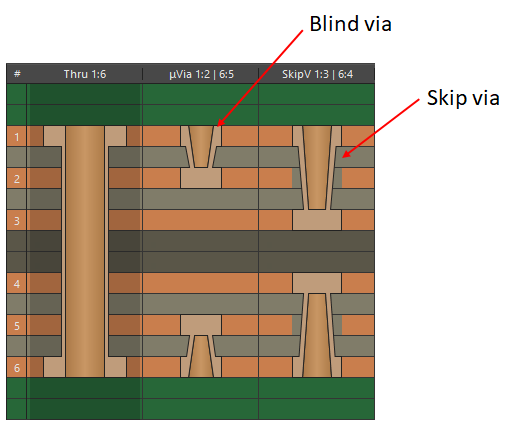
Skip Vias
Skip vias appear in Type 1 HDI stackups and in non-standard stackups. The use of skip via's is intended to reduce a process step on an internal drilling layer. While eliminating one drill step in the sequential buildup process reduces costs, it reduces the routing flexibility, especially when routing will be very dense on multiple layers.
Blind via and skip via side view
The depths of skippedia's, in terms of the number of layers they skip, is also limited by layer thickness and aspect ratio. Once again, contact your fabrication house and get there the sizing requirements before designing skip Vias.
Every-Layer Interconnect (ELIC)
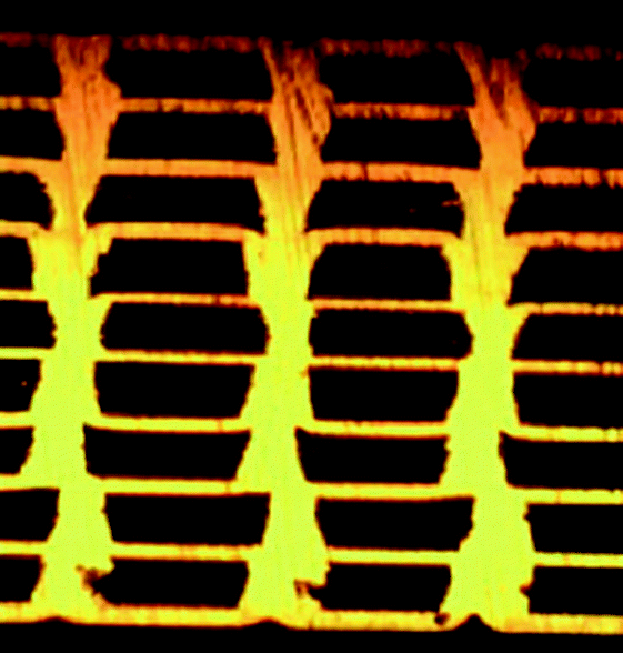
The point of ELIC is to take stacking of blind and buried microvias to its logical conclusion: to stack these throughout the entire HDI stackup. This requires that internal core layers be very thin in order to fabricate an appropriate stack with a buried via as the central core transition. This is in contrast to one of the other standard HDI builds, where the thick internal core uses a conventionally drilled buried via for some internal layer transitions.
Microsection image of ELIC via transition. Read more here.
ELIC stacking of blind and buried vias allows the vertical layer transitions to take up the least amount of space. This also uses sequential buildup through the entire PCB stackup, and it will be the most expensive fabrication process. This is because every layer in the design must be drilled individually, followed by sequential lamination of the fabricated layers.
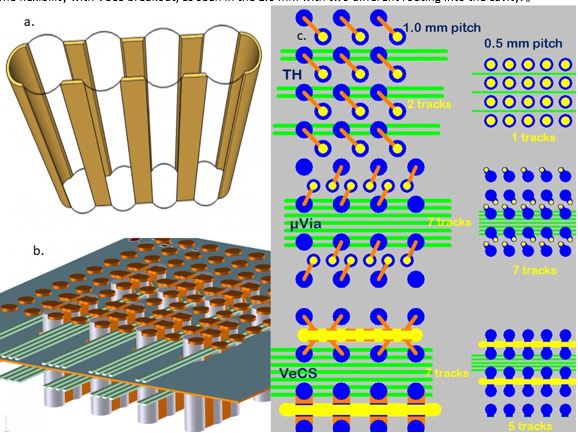
Vertical Conductive Structures (VeCS)
Many fabrication houses are standardizing ELIC transitions, but VeCS is more specialized. In VeCS, a plated hole is milled such that there is a small cutout in the pcb. The remaining sidewall forms a copper plated vertical transition into an internal layer. This type of layer transition was originally discussed by Happy Holden in this linked article.
Happy Holden’s excellent illustration of VeCS.
Since this adds yet another step to fabrication, why should this vertical transition be used?
The inductance and capacitance characteristics of this type of transition are completely different from a standard via. This is because we no longer have a cylindrical structure, and instead we have a vertical structure that is much smaller. There may be signal Integrity benefits that come with this type of structure due to the change in geometry. This is particularly the case in vertical interconnects operating at very high frequencies, where engineering an antipad in the surrounding dielectric is very difficult. If signal Integrity is the reason behind the use of the structure, it should be simulated in a 3D electromagnetic field solver.
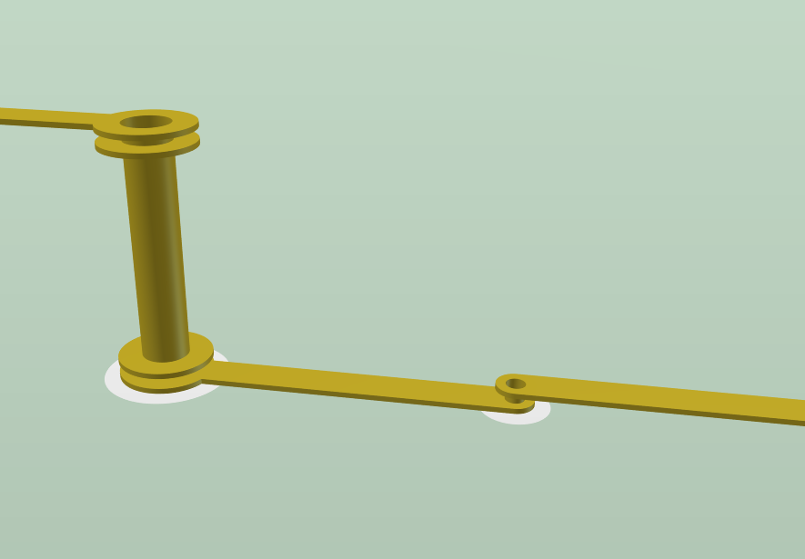
Boomerang Vias
In a type 2 stack, or in a non-standard stack up with through-holes, you will sometimes need to route almost totally across the board while avoiding the influence of stubs. Stubs on the top side and bottom side of a PCB can be eliminated by combining blind/buried vias, or a skip via, with the through-hole via that traverses the PCB layer stackup. An arrangement known as boomerang vias can be used to make this transition.
With a boomerang via, you route down the through-hole to pass the entire layer stack, and then back up through blind/buried vias to the destination layer. This eliminates stubs on the route, with the trade off being that it slightly increases the routing distance. Depending on the bandwidth, eliminating stubs would be preferable to slightly increase insertion loss as it ensures the channel bandwidth stays large enough for your signaling specification.
Boomerang via illustration in 3D
Talk to Your Fabricator First
Before using any of these layer transitions, make sure to contact your HDI PCB fabrication house. They can provide guidance on the geometries to use in these PCBs, as well as the layer stack that will ensure reliability.
Keeping up with microvia technology and newer innovations in HDI routing takes the complete set of PCB design features and world-class CAD tools in Altium. To implement collaboration in today’s cross-disciplinary environment, innovative companies are using Altium to easily share design data and put projects into manufacturing.

About Author
Related Resources
Related Technical Documentation
Table of Contents
Design to Release, Without the Friction
- Keep reviews tied to the right version
- Reduce handoff confusion and rework
- Spot sourcing and release risk earlier
- Work solo, share when needed
Get Started
Thank you, you are now subscribed to updates.

