Comparing Static and Dynamic Flex Design: Rigid Flex PCB Bend Radius and Other Mechanical Considerations


Like it or not, flex and rigid-flex PCBs are here to stay, and progressively more flexible electronics are moving out of the research phase and into industry. Flex PCBs are now used for much more than powering a motor in your magnetic hard drive. Any device that contains a foldable or translating element likely includes a dynamic flex PCB.
With the growth in the flex PCB market reaching tens of billions, PCB designers have every incentive to learn as much as they can about both static and dynamic flex PCB design. Your company’s next product or a redesign of an existing product may depend on it.
Static vs. Dynamic Flex PCBs
Any flex PCB is related to a rigid-flex PCB in that they use the same materials for the flex layer. Rather than having rigid sections with polyimide core surrounded by copper and prepreg, a flex PCB is constructed entirely from a flexible material. Polyimide is typically used as it is easily adaptable to rigid-flex manufacturing processes and is relatively inexpensive, although polymer materials like polyethylene naphthalate (PEN ), polytetrafluoroethylene (PTFE), and Aramid can also be used for flex ribbons.
Flex PCBs can be designed as dynamic or static PCBs. Designing either type of flex PCB is as much a mechanical exercise as it is an electrical exercise. PCB design software with ECAD/MCAD collaboration features are great for designing either type of flex PCB. When planning a stackup and placing traces flex PCBs, the bent section of the board should be treated as a bent rectangular plate during mechanical analysis. This is vital for determining the right trace thickness in order to prevent cracking and failure.
Whether you are designing a static or dynamic flex PCB, a thicker overall flexible stackup requires a larger bending radius. This reduces the amount of tensile and compressive stress from concentrating along the bend while forming the PCB to the desired angle. Placing a smaller bend radius in a thicker PCB can cause the coverlay to bunch at the surface layer inside the bend. This then puts more compressive shear stress on the traces that lie inside the neutral bending axis. If you want to reduce the overall thickness, there are flexible coverlays available that do not require an adhesive.
Static Flex PCBs: Manufacturing Considerations
Once a static flex PCB is manufactured, it is usually bent during assembly to the desired radius of curvature and bend angle with a compressive forming tool. This tool acts like a vise, and customized forming tools can be used to place multiple bends in a single flex ribbon simultaneously.
Static flex PCBs are typically overformed beyond the yield point, meaning they are bent beyond their intended bend radius in order to ensure some plastic deformation during forming. This prevents the flex PCB from relaxing back to its original shape once it is removed from the forming tool. When the static bending radius and angle are specified in a static PCB, you should actually plan to have a margin of safety in your trace thickness in order to prevent hairline cracking and failure during overforming.
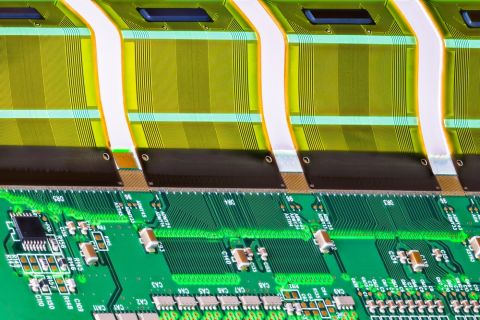
Static flex ribbon for a medical device, as featured in Electronics Weekly.
Intuition might state that the traces should be thicker in order to withstand the stress required during overforming, but intuition is not always correct. Simply put, the thicker the circuit, the less it can flex without damage. Thicker flex PCBs will require greater overforming to conform to the desired bend radius and angle. This places even more stress on traces during forming.
Just like a bent rectangular plate, there will be a neutral bending axis throughout the flexed board, which defines a curve along which there is no longitudinal tensile or compressive stress. Thinner traces can withstand greater compressive stress than tensile stress, so thinner traces can be placed inside the neutral bending axis. The shift in the neutral bending axis will depend on the bending radius. A good rule of thumb for the minimum bend radius is to use the following equation:
If the stackup and trace thickness are chosen properly, following this rule will ensure that the neutral bending axis will not shift appreciably from the centerline of the PCB. As the layer count increases, this will ensure that you comply with the IPC 2223C standards on the bending ratio (bend radius divided by thickness) in flex PCBs.
Dynamic Flex PCBs: Durability
Many of the same design considerations for static flex PCBs also apply to dynamic flex PCBs. A critical problem in dynamic flex PCBs is work hardening during repeated bending. Copper will work harden under repeated cycling, eventually becoming brittle and prone to fracture. The durability can be extended by simply allowing for a larger bending radius. It is generally advised that dynamic flex PCBs not exceed a 90° bend angle.
As the PCB bends, the neutral bending axis will shift towards the interior of the bend. This is very important in dynamic flex PCBs as it limits the number of allowed copper layers to a low number, typically only a single layer that coincides with the neutral bending axis. Although copper is ductile, it will work harden when repeatedly placed under stress. If you do opt to use more than one layer in a flex PCB, the traces should be staggered, i.e., they should not overlap in adjacent layers, in order to avoid undue stress on traces farther from the neutral bending axis.
To prevent undue stress on traces, be sure to allow a sufficient margin of safety and pay attention to the minimum bend radius. Make sure that the minimum bend radius is smaller than the intended bend radius in order to prevent stress at the edges of the board. This will slow work hardening and help extend the usable life of the PCB.
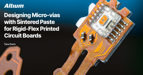
Static flex ribbon for a hard drive
As flex PCB design continues to make inroads in more devices, designers need software for flex PCBs that eases layer stack design, production planning, and more. Altium Designer provides these important design tools, MCAD tools, and much more in a single unified design interface. The intuitive design interface and rules-driven design engine is easily adaptable to rigid, rigid-flex, and fully flexible PCB design.
Now you can download a free trial of Altium Designer to learn more about the layout, layer stack management, and production planning tools. You’ll also have access to the industry’s best signal integrity and documentation features in a single program. Talk to an Altium expert today to learn more.

