

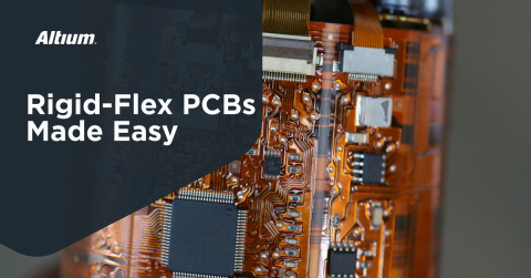

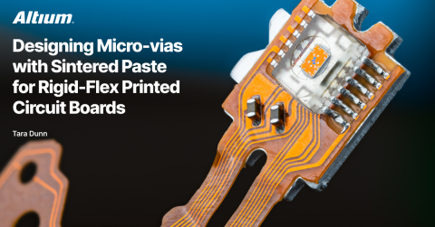


Flex Circuit Design Guide: Getting Started with Flexible Circuits

At a Glance
Get started with flex circuit design. Learn key considerations, materials, and best practices for designing flexible and rigid-flex PCBs.


Speaking to a group of students about printed circuit board fabrication recently, I asked for a show of hands, asking how many had designed a rigid printed circuit board. Roughly 75% of the room raised their hands. The follow-on question asked for a show of hands for those who had designed a flexible circuit. The number of raised hands dropped dramatically. I suppose this shouldn't be surprising. While flex circuits are a growing segment of the printed circuit board industry, many seasoned PCB designers have not yet worked with flex materials. Thinking back to my college days, I think my knowledge of flexible circuits extended only as far as "that white ribbon that moves back and forth in my printer."
Those flexible circuits on polyester are certainly a significant portion of the flex market. There is no denying the volume driven by RFID tags, which often use aluminum on flexible polyester materials. However, when I am asked to speak about flex circuit fabrication or design, it is nearly always addressing the market segment utilizing flexible polyimide materials. These materials are standard in the flex and rigid-flex world as they integrate with a PCB stackup, allowing simplified routing between rigid and flexible regions with standard interconnects. In this guide, we'll look at how flex PCBs are made, starting with design and covering the various materials and processes used in fabrication.
The Flex PCB Design Process
Flex PCB and rigid-flex PCB design and layout are interrelated; the major difference between flex and rigid-flex is an interconnect spanning into the rigid ends of the board. Much like a standard rigid PCB, the flex design process starts with designing a stackup, placing components, planning and routing paths for traces, and finally cleaning up the layout to prepare for manufacturing. Some additional steps are required to ensure the flex section has the required mechanical properties, such as adding a stiffener, selecting a coverlay or photoimageable solder mask material, or setting a static bend in the design.
Because so much of the flex ribbon design process centers around the stackup, as well as its integration with any rigid section, stackup design is a critical part of the flex/rigid-flex PCB design process. In addition, things like copper weight and component/routing density in certain regions of the board can limit flexibility, making a rigid-flex board preferable. To get started with a flex or rigid-flex design, think about the following aspects of the final assembly and how the design will be integrated into its enclosure:
- Floorplanning: Where does the flex ribbon need to bend in the PCBA, and how will the design mount into its enclosure? The bending and mounting areas will need to be free of components, and you might want to use a rigid section for certain high pin-count ICs or high density circuitry. Decide where the flex ribbon will sit with respect to areas of the board with high component count.
- Layer count: How many layers are needed for routing, and will some of these layers be needed in a rigid section? If there is a rigid section, the flex ribbon will need to fit in the center of the stackup, which can make routing difficult when a larger number of planes are required (e.g., in a high-speed design).
- Stiffness: Can you accept a stiffer board, or will you need a highly flexible assembly? This can be controlled with component density, copper weight, or the addition of stiffeners to certain portions of the flex ribbon. If you need a very stiff polyimide section, it might be worth placing a fully rigid section instead. Stiffeners can be used to support higher component density on a flex ribbon, and they will be less expensive than integrating a rigid section.
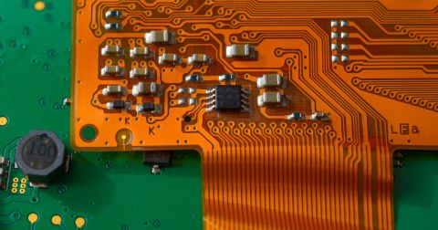
- High-pin density components: Smaller SMD components like passives can be easily placed on a polyimide flex ribbon. Other components in BGA packages require a more advanced via structure, as well as more internal layers to support routing. For high-speed or RF designs, hatched plane layers may be needed to provide required impedance or ground continuity (e.g., for single-ended signals), as well as isolation.
Your application requirements could dictate balancing any number of these requirements. Meanwhile, designers need to ensure their rigid-flex or flex design is manufacturable and will be reliable in the field.

Materials for Flex/Rigid-Flex PCBs
Once you have decided to move ahead with a flexible circuit design, what are the key items to keep in mind? We will review these in more detail in future blogs, but you'll need to consider your material set in order to get the process started. The materials required for flex PCBs include base materials (polyimide, copper foils), coverlay materials (polyimide or liquid photoimageable), and, finally, stiffener materials.
Flexible Base and Coverlay Materials
It is crucial to understand the base materials themselves as well as the coverlay. Will your application require adhesiveless materials? Or adhesive-based materials? Does the application have any UL requirements to consider? What copper weight and polyimide thickness is best for your application? What materials does your fabricator routinely stock? (Hint: if you have flexibility in materials, routinely stocked flexible materials can help keep costs down)
Some applications will best be suited to flexible liquid photo imageable coverlay, which offers the ability to form very tight pad openings. If the design requires dynamic flexing, the application should use a film-based polyimide coverlay material. Film-based could have either laser-cut openings or drilled openings, depending on the required pad size.
Stiffeners
Will your application be supporting heavier components and could benefit from the robustness of an added stiffener? Different components and applications need different stiffeners to support mechanical behavior in the flex ribbon or PCBA. Common stiffeners include:
- FR4 stiffener: Rigid FR4 epoxy-impregnated fiberglass is probably the simplest stiffener, effectively applied as a laminate over the flex area.
- Rigid polyimide: A rigidized polyimide layer can be used to stiffen a region by simply stacking additional polyimide sheets to produce a local thickness increase. This is normally used when terminating with a ZIF (Zero Insertion Force) connector, where a polyimide stiffener is used to build to the appropriate thickness.
- Connector/component stiffeners: Material options for this application include metals, FR4, or polyimide, which are thermally bonded with a flex adhesive or pressure-sensitive adhesive.
Flex and Rigid-Flex Stackups
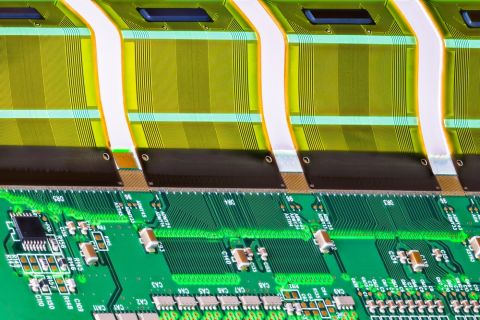
Flex and rigid-flex PCB stackups mix the above materials into flex and rigid regions, either as single-layer or multilayer boards. Multilayer PCBs built on flex substrates follow somewhat different design rules in terms of how to interface with the rigid section, how to route in the flex section, and where components can be placed. Flex PCB stackups typically build up a layer stack using overaid adhesive-copper-adhesive layers, followed by lamination into a rigid stack with prepreg, or topping with a coverlay layer to protect the lower flex polyimide layers. An example of a flex PCB stackup, including two rigid sections on each end, is shown below.

In the above image, we could build the same type of flex stackup without the rigid section, generally following the same process. The difference is in the omission of the rigid sections that bind the flex regions together. Instead, we would have all flex materials topped with coverlay. There is even solder resist that can be used on flex PCBs to protect the top/bottom coverlay layers during soldering.
Fabricators' Capabilities
Do your existing preferred fabricators work with flexible materials on a regular basis? Will the complexity of your design match well with your preferred fabricators' capabilities, or are you stretching beyond their area of expertise? This is certainly not an all-inclusive list of things to consider but is intended to start the thought process of designing with a flexible circuit. Your PCB fabricator will be a vital resource, and you should contact them with a proposed stackup to ensure it can be reliably fabricated. They understand the materials and the fabrication process and will always be happy to help guide a customer along the learning curve with flexible PCBs.
Benefits of Flex PCB and Rigid-Flex PCB Designs
For those who are not experienced in flexible circuit design, let's look at a few of the key benefits driving designers to use flexible materials. Although there are some particular design considerations needed to ensure a flex or rigid-flex PCB design is manufacturable as intended, these designs provide many benefits that aren't seen in rigid circuit boards.
- Space and weight: Many of today's electronic designs are challenged to reduce the size and weight of the end product. Flexible materials can replace bulkier wire and solder connections, and a frequently touted statistic places that savings as high as 60% in the right circumstances. That is significant.
- Packaging Benefits: There is no denying that the ability to bend and fold a flexible circuit around a corner and the ability to provide a three-axis connection gives the PCB designer a significant advantage over both traditional wire and cable and rigid printed circuit board materials. In fact, the ability to best take advantage of these benefits is limited more by the imagination than anything else.
- Simplified Assembly: When compared with bulky wire and cable, a simple, flexible circuit can dramatically shorten the assembly effort. One flex circuit can replace multiple line items on a bill of materials.
- Thermal Management: Polyimide materials can withstand high heat applications, and thin polyimide dissipates heat much better than thicker, less thermally conductive materials making this a top contender for higher power, higher frequency designs.
- Biocompatibility: Polyimide and LCP are two flexible materials that are an excellent choice for biocompatibility and are regularly used for that reason in both medical and wearable applications. Interestingly, I have been seeing increasing interest in flexible circuits that use gold as a conductor rather than copper, providing a fully bio-compatible option.
After fabrication, the flex portion of the circuit board assembly can be placed in its enclosure with static bending, or it can be allowed to flex dynamically with the enclosure or other mechanical elements. Sometimes, a flexible circuit is designed to be "flex to install" or, in other words, bent or folded with the intention of remaining stationary once the circuit is installed into the final electronics. Other times, the application requires a circuit to be flexed hundreds, thousands, or even millions of times. Disk drives are a commonly touted example of a dynamically flexing application, as are the flexible circuits in the hinges of our laptop computers. The design process varies slightly with static and dynamic flex assemblies, with the major consideration being deformation that can occur during bending.

Flex and rigid-flex PCB design engineers, layout engineers, and SI/PI engineers trust the advanced design tools in Altium for their design and layout needs. When you've finished a design and are ready to release it to manufacturing, Altium makes it easy to collaborate and share your projects. Altium also integrates with popular MCAD and simulation applications, giving you the ability to better understand power and signal behavior in multi-board systems.
Have more questions? Call an expert at Altium and discover how we can help you with your next PCB design.
About Author
Related Resources
Related Technical Documentation
Table of Contents
Design to Release, Without the Friction
- Keep reviews tied to the right version
- Reduce handoff confusion and rework
- Spot sourcing and release risk earlier
- Work solo, share when needed
Get Started
Thank you, you are now subscribed to updates.

