Flexible Circuit PCB Stiffener Options


Why Would I Need a PCB Stiffener For My Flexible Circuit Design?
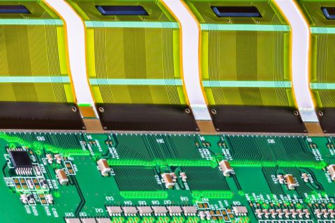
Fundamentally, the benefits of using a flexible circuit in a design are the ability to bend and fold the circuit and to allow the circuit to flex during use. These thin and flexible stack-ups solve a considerable number of packaging issues. But, being thin and flexible can also present a few challenges. It is common for a flexible circuit stack-up to include a PCB stiffener, which is typically going to be either a layer of polyimide or a layer of FR4 material, to provide added support and rigidity in specific areas.
FR4 PCB Stiffeners
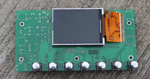
An FR4 stiffener is most often used to support a connector area. If there is a heavy connector, or at least heavy in relation to the weight of the flexible circuit, a piece of FR4 can be applied to the flex in that area to provide stability and prevent damage to the copper traces. FR4 stiffeners are also used to support areas in the design that have a number of smaller, or lighter components and the PCB stiffener functions both as a support for connector weight and to prevent bending or flexing in that area, which could put stress on the solder joints.
An FR4 stiffener could simply be a piece of FR4 with copper removed used as a backer to the flex area, or it could have drilled holes and be registered to the flex to allow for thru-hole components. Sometimes, this “stiffened” flex is confused with a rigid flex construction. There is one significant difference between a rigid flex and flex with a rigid stiffener PCB; as a stiffener the FR4 is functioning only as a mechanical support, there are no plated through holes providing electrical connection between the flex and the rigid material.

FR4 PCB stiffeners are added to the flexible circuit as one of the final fabrication steps and can be applied with either a layer of pressure sensitive adhesive or a layer of thermal set adhesive. That decision may be driven by end-use or fabricator preference. From a low-cost perspective, if the end use is not in a particularly harsh environment, the pressure sensitive adhesive application will most often be slightly less expensive. Thermal set adhesive requires the flex to be placed back in the lamination press to apply the heat and pressure needed to cure the adhesive. The extra time and labor can add cost. As a cost-saving tip, keeping all the stiffeners the same thickness reduces processing time in fabrication and helps to keep the cost down.
Polyimide PCB Stiffeners
Polyimide stiffeners in PCBs have many different functions. They too, can add rigidity to a component area and prevent bending and folding that could put stress on solder joints. Polyimide PCB stiffeners can be utilized for other functions as well. One typical use of a polyimide stiffener is to match a mating thickness requirement for insertion type connectors. ZIF connectors are a common connection method with flex designs. These connectors have a specific thickness spec and tight tolerance on that thickness to ensure the connection is effective. A piece of polyimide can be added in that area to build the stack-up to the required thickness, while allowing the rest of the flex to remain thinner and more flexible. A general rule of thumb to keep in mind is to be sure the PCB stiffener and coverlay end points overlap by at least .030” to avoid introducing a stress point in the flex design.
Polyimide stiffeners also perform other functions. For example, if a flex circuit is going to have something rubbing up against it in end use, a layer of polyimide can be added to that area, so the wear and tear is being done to the non-functional piece of polyimide rather than directly on the circuit itself.
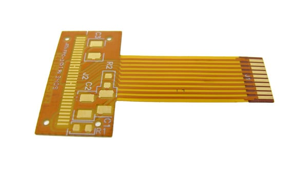
Polyimide stiffeners in PCB designs can also be used to adjust the natural bend area in a flex as it is installed or to create a bend in a specific location. For example, as the flex is installed, if there is a natural bend area that is interfering with another piece of the unit, adding a layer of polyimide will adjust that natural bend area to a more desirable location. As another example, certain applications benefit by adding polyimide pieces on either end of a bend area to both ensure the bend is being done in the proper location and to help operators clearly understand where the flexing and bending need to happen. The locations of polyimide stiffener placement in PCBs can be easily customized.
Polyimide stiffeners can also be applied with both pressure sensitive adhesive or with thermal set adhesive. Unlike FR4 stiffeners, polyimide stiffeners are often applied in the same lamination process step as the polyimide coverlay. This eliminates an extra process step for the PCB stiffeners themselves. In fact, if pressure sensitive adhesive is called out, it can often add cost due to additional processing being required. Later in the process, the areas with polyimide stiffener are punched or routed along with the circuit outline eliminating any registration concerns.
To Answer the Original Question...
In a flex circuit PCB design, stiffeners have many functions. The most common is to provide support to a connector area, either for concerns with the weight of a component or to support a component area and eliminate stress on solder joints. Insertion connector areas typically require an added layer of polyimide to build that area to the specified mating thickness. Beyond those common uses, PCB stiffeners can be used to build up a wear area in the end use and adjust the bend locations in the final installation.
Have more questions? Learn everything you need to know about flex and rigid-flex design in our free ebook. The next time you're searching for ECAD software for your flex PCB designs, look no further than Altium Designer®. When you’ve finished your design, and you want to release files to your manufacturer, the Altium 365™ platform makes it easy to collaborate and share your projects.
We have only scratched the surface of what’s possible with Altium Designer on Altium 365. Start your free trial of Altium Designer + Altium 365 today.
