


Do You Always Need 1 oz. Copper Thickness on Each Layer?

At a Glance
1 oz. copper thickness is often seen as a standard thickness value used in many designs. Here’s when you might need thicker copper on every layer.


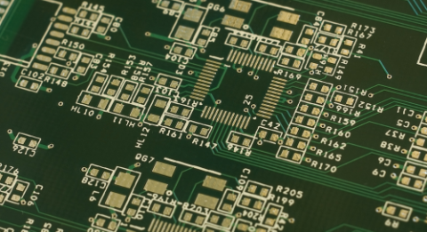
If you ask your fabricator for a standard PCB stackup, you’ll likely see 1 oz. copper plating (~35 micron or 1.4 mils thickness) on the outer layers as well as inner layers. Is this the right value from a manufacturability perspective, or should you use an alternative copper weight on different layers? There are several variables to consider here, ranging from voltage and current requirements on certain interconnects, as well as resin content of your dielectric and the material system you plan to use.
Using 1 oz./sq. ft. copper weight on each layer is an easy choice if your fabricator recommends it, but some designers might get the idea that an alternative copper weight might be better for their application. Rather than look at specific applications of different copper weights, we’ll look at some considerations around using alternative copper weights, as well as mixing copper weights in different layers. Manufacturability is key here as copper weight determines important parameters like allowed trace density and required laminate resin content.
Matching Copper Weight, Layer Thickness, and Processing
PCB fabrication houses will give you a specific copper weight in their stackups for a particular reason: processability. Fabrication needs to pair up laminates with particular copper weight, resin content, and dielectric thickness values to ensure a design can be fabricated reliably. Standard stackups are the starting point for a lot of designs, but these aren’t the only options you have available.
Although fabrication houses give standard stackups that they know will pass through processing, you’re still free to propose a stackup for your circuit board. However, you shouldn’t assume that you can just pair up any dielectric materials, copper weight, and resin content you want. You’ll be limited by what laminates are actually produced by materials vendors, as well as the overall board thickness requirements.
Obviously, try to match up your copper thickness requirements with your target application if you want to use something besides 1 oz. copper. To see when different thicknesses might be required for various applications, take a look at this article. If you know you’ll need non-standard copper or heavy copper, here are some considerations for fabrication:
Heavy Copper on Internal Layers
If needed, you can select heavy copper for internal layers, but just note that the fabricator may set a limit on the maximum copper weight. Some limits can go ridiculously high, like 10 oz. or higher. However, be careful with trace routing using heavy copper; the potential problem is one of bond strength between layers. When layers are pressed, excessively thick copper can leave some voids around it where resin does not flow, which creates a weak spot around thicker, narrower traces.

This is solved by having higher resin content in the dielectric. Higher resin content will allow more resin to flow during pressing, which will fill in those voids. Your fabricator should be able to qualify your copper weight selection in their process. Since heavy copper is often used in high current, one option is to forego thicker copper and just use wider traces to hit your DC resistance target. Keep this in mind when considering heavy copper in internal layers.
Etch Compensation and Spacing
If you use heavier copper, the etch time will be longer, which means more etch compensation will be required to ensure the target trace width is produced on the board. Etch compensation is used to account for the fact that a trace width on a layer will be slightly smaller than the design value due to the etching process during fabrication. This will always happen, and it’s one of the reasons there are required clearances between traces on a board. Because heavier copper requires longer etching time, it will also require greater etch compensation and larger spacing between traces to prevent shorts.

Fabricators don’t always provide specific etch compensation numbers, and they will instead roll this requirement into their minimum trace-to-copper clearance values. I have seen only one table from an overseas manufacturer that provides some specific etch compensation values for 1 oz. copper thickness and heavier copper films. As a designer, make sure you follow clearances in the layout by defining them in your design rules.
Starting vs. Finished Plating Thickness on External Layers
The last point to consider here is what actually happens in the manufacturing process. When you specify that you need 1 oz. copper plating thickness (or some other standard value), you should be clear that this is the finished plating thickness. Remember, during the fabrication process, your board will pass through etching and the initial copper on the surface layer will decrease in thickness over time. Eventually, the exposed conductors will have some plating applied, which will fill out exposed copper to the desired thickness value.
If you fill out the quote form on your manufacturer’s website, they will generally be asking for the finished plating thickness you need in your bare boards. Good manufacturers will ask you explicitly for the finished plating thickness on the quote form, or they will explicitly call out a finished copper weight in their standard stackup. Therefore, when you prepare PCB fabrication notes and specify copper thickness values in your PCB stackup, it doesn’t hurt to call this out as the finished plating thickness.

The final plating thickness will be determined by the fabricator. Just as an example, for electroless nickel immersion gold (ENIG), the typical plating thickness can be up to approximately 5 microns. However, you don’t need to specify this; your fab house will handle this for you within their process.
If you need a different plating thickness, but you want the reliability of your fabricator’s standard processing, just make sure to check with them for their standard stackup requirements. Some fabricators will do non-standard processing down to odd copper weight values, including as small as 0.25 oz./sq. ft. copper weight. Just make sure to clearly specify the value you need for your PCB stackup when you’re consulting with fabrication houses.
If you’re designing with something other than 1 oz. copper thickness, or if you want to create your PCB stackup with an alternative copper thickness, use the PCB design tools in CircuitMaker. All CircuitMaker users can create schematics, PCB layouts, and manufacturing documentation needed to move a design from idea to production. Users also have access to a personal workspace on the Altium 365 platform, where they can upload and store design data in the cloud, and easily view projects via a web browser in a secure platform.
Start using CircuitMaker today and stay tuned for the new CircuitMaker Pro from Altium.

About Author
Related Resources
Related Technical Documentation
Table of Contents
Design to Release, Without the Friction
- Keep reviews tied to the right version
- Reduce handoff confusion and rework
- Spot sourcing and release risk earlier
- Work solo, share when needed
Get Started
Thank you, you are now subscribed to updates.

