


Selecting Materials for High Voltage PCB Design and Layout

At a Glance
Your high voltage PCB design will need a board material that’s specifically designed to tolerate high voltages, as well as potential for overvoltage and high temperature.


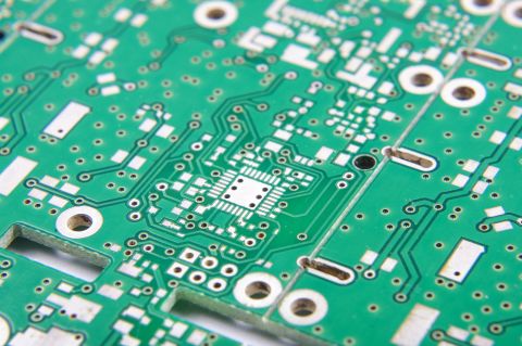
Somewhere below all the components in the above image is a PCB made from rigid stackup materials, and these materials must meet certain operating standards in order to meet basic performance needs. Something that many newer power electronics designers will do, including high voltage power systems designers, is to just request the default stackup from a fabricator and start creating the PCB layout immediately. This is a perfectly acceptable (and often recommended) practice for many generic products; examples include smaller microcontroller boards.
So what’s wrong with taking the same approach for a high voltage PCB material?
High voltage PCBs are subject to certain safety and reliability concerns that you won’t find in most other boards. If your fabrication house specializes in high voltage PCBs and keeps materials in stock, they can likely recommend a material set, as well as a standard stackup you might use for certain voltage ranges and frequencies. If you need to choose your own materials, follow the tips below to help you narrow down to the right material set.
Choosing the Right High Voltage PCB Materials
When we’re referring to “high voltage”, we’re usually talking about something reaching into the kV range, either in DC or AC. There are a few material properties in laminate datasheets that can help you determine which laminates are best for your circuit board and will ensure reliability at high voltage. Some example substrate materials used in high voltage PCBs include:
- BT epoxy
- Phenolic-cured rigid laminates
- High voltage teflon (HVPF)
If you want to use a different material set, pay attention to these specifications:
Comparative Tracking Index (CTI)
One of the important summative metrics used to quantify the ability of a design to withstand dielectric breakdown is its comparative tracking index (CTI). The CTI defines the voltage at which an insulating material like a PCB substrate begins to break down near the surface. During breakdown, the material begins to carbonize and becomes more conductive, which increases leakage current and accelerates breakdown over time.
Industry standards such as IEC-60950-1 and IPC-2221 mention some recommended materials for high voltage PCBs based on CTI values. These values can also be determined using some standard tests, most notably with either UL 746A, IEC 60112, or ASTM D3638. CTI values are classified in six Performance Level Categories (PLC):
|
|
|
|
|
|
|
|
|
|
|
|
|
|
|
|
|
|
|
|
|
In effect, CTI gives you a way to estimate the leakage current between two conductors when the conductor spacing becomes very small. One should note that the degradation being captured with CTI is not the same as dielectric breakdown leading to ionization and subsequent current surge. These ratings are much higher than the CTI rating, typically on the order of kV. Designs exposed to these voltages will need, at minimum, a PLC 0 material to ensure long-term reliability.
Resin Content, Glass Weave, and Curing Agent
The material system used in the design, specifically the resin content and curing agent, will influence the reliability of the design. FR4 laminates can be used at the lower end of what would be considered high voltage PCB design as they have low CTI values (~200-300 V DC) despite their high breakdown voltage values. The resilience of a high voltage PCB material over time is related to both the resin content and the curing agent. There are two reasons this is important in a high voltage PCB:
- Conductive anodic filamentation (CAF) failure, where high voltage encourages metal migration and electrochemical growth of dendritic structures between conductors held at high potential.
- Voids at low resin content, which will increase the chances of degradation mechanisms between layers in the PCB stackup. Higher resin content is generally preferred in high voltage designs, which means the fiber weave will be looser.
In dicyandiamide (DICY)-based FR4 laminates, the glass transition temperature (Tg) value can be rather high, reaching around 180 °C. However, these resin systems can fail earlier at high voltage gradient, as data from Isola shows (se below). While both might offer similar CTI, the failure rate with the phenolic curing agent is longer as CAF growth is inhibited in the cured laminate.

Another aspect of reliability in high voltage boards is the glass weave. Somewhat finer glass weave like 1080, 2113, or 2116 would be ideal, while something as loose as 106 weave could experience reduced long-term lifetime. These weaves still allow resin flow and penetration while balancing the need to inhibit CAF at lower voltages.
Surface Finishes and Copper Weight
You will also want the quality of your copper to meet your high voltage operating requirements. This involves selecting copper weight and a surface finish. Whether you're using bare copper (not recommended) or a standard surface finish like ENIG, the finished surface should be as smooth as possible. Designs with smoother surface finishes are preferred as a rough interface creates areas where static charge can accumulate. At low voltage, this is not really a problem as the field strength between various sections of a conductor will be too low to cause arcing or dielectric breakdown in air. You fabricator should be able to provide guidance on this point with respect to handling finished boards and the best plating material/thickness for your required copper weight.
Copper weight becomes more important when we look at high current materials, which is something that tends to occur alongside high voltage, although this is not always the case. Copper weight should be higher when current is higher, and at some point you will need to switch to busbars when currents exceed ~100 A in a large layout. The IPC-2152 nomograph is a good place to start sizing conductors for your PCB, although just note that the values recommended in that standard can be overly conservative and are not universally applicable to all PCBs.
Starting Your High Voltage PCB Layout
At the end of the day, you're choosing laminates that will support your board and can survive long-term high-voltage operation. Once you have the laminate layers, copper weight, and plating for your PCB sorted out, you can move on to planning your stackup and PCB layout. The stackup should be created in consultation with your fabricator, who will normally be able to suggest an alternative laminate if your specific laminate is unavailable.
Next you'll want to ensure your layout will obey basic safety and reliability rules, which involve spacing between conductors as dictated by safety standards. IPC-2221 will be the starting point for most PCB layouts on rigid boards. Alternatively, for something more reliable like mil-aero electronics, MIL-STD-275 recommends setting spacing to 8 V/mil, although some of these standards are older and haven’t been updated to account for new materials like HVPF or Kapton that can handle 1000 V/mil. Pay attention to these PCB standards and other industry-specific standards (e.g., IEC) for more guidance.
Once you've found your materials and it's time to start your new high voltage PCB layout, use the best ECAD software in Altium. When you’re ready to release these files to your manufacturer, the Altium platform makes it easy to collaborate and share your projects. Everything you need to design and produce high voltage PCBs can be found in one software package.

About Author
Related Resources
Related Technical Documentation
Table of Contents
Design to Release, Without the Friction
- Keep reviews tied to the right version
- Reduce handoff confusion and rework
- Spot sourcing and release risk earlier
- Work solo, share when needed
Get Started
Thank you, you are now subscribed to updates.

