


PCB Stackup Basics

At a Glance
How to assign layer types in a PCB? Expert Phil Salmony shares with us some of his favorite multilayer stackups, complete with guidelines.


In comparison to the build-up of a PCB, the stackup is more concerned with the electrical type of each layer. Material thicknesses or what dielectrics are used is of less importance than which layers are dedicated to what, such as signal (SIG) layers, ground (GND) layers, or power (PWR) layers.
Signal layers contain predominantly signal-carrying traces (sometimes with routed power or copper pours), whereas power and ground layers are typically completely solid copper pours over the entire layer. Ground layers are used for reference of the signal layers and their return paths, and a power layer is either a solid, continuous power plane of a certain voltage or several islands or copper pours of various different voltage levels.
Before routing a PCB, we want to determine our stackup, which depends on the number of layers we have available. Then, we want to go through the layers one-by-one, assigning ground, power, or signals to individual layers.
Combinations are of course also possible—we can mix power and ground, signal and ground or signal and power.
Ground Layer
One of the most important layer types is the ground layer. This layer type is used predominantly as a reference plane or layer for signal (and power) trace return paths. For every forward path, we need a return path to complete the loop.
Power Layer
A power layer is used for power distribution. Keep in mind that for low-speed and low-bandwidth systems it isn't entirely critical, and you can route your power with traces on signal layers. However, power planes and layers become increasingly important in terms of power delivery for high-speed circuits. Additionally, if coupled with a ground layer on a closely spaced, adjacent plane, these form a type of parallel plate capacitor.
Signal Layer
Lastly, we have our signal layer where we will route our traces, effectively forming our signal forward path. As seen before, we can use a ground layer or in certain cases even a power layer as a reference for our return path.
Return Paths and References
Now the question is, how do we assign layer types in a PCB in a sensible way? We have certain goals for EMI performance, signal and power integrity, and we want a systematic approach to deciding the stackup. We don't want to just arbitrarily assign different layer types.
There are a couple golden rules. Firstly, for AC signals in the region of a couple of kHz, the return path is not the shortest path but rather the path directly underneath the trace (forward path). This is the part with the least impedance. For example, for a trace on a top signal layer and a ground plane directly below on layer two, the forward path is on the signal layer, and the return path is directly below that trace in the ground plane beneath.
Another thing to consider is that the signal energy flows in the dielectric space between the copper (trace and plane). The copper therefore is simply a waveguide. For good signal integrity and EMI performance, we need to take into account both the forward and the return path, where the signal energy is flowing, and how it is bound between the forward and return paths.
In essence, close couplings between signal and ground planes and power and ground planes is desired in order to prevent fields from spreading. Our main goal is to avoid fields from spreading, as spreading fields lead coupling from signals to signal, which leads to crosstalk. Spreading fields also mean some form of radiation, which leads to EMI issues.
Assigning Layers and Layer Pairs
How do we avoid fields from spreading, and how do we contain these fields?
The main thing we as PCB design engineers need to keep in mind, is that every forward signal or power path needs a closely coupled reference. In addition, for high-speed or higher-energy signals, it makes sense to also use stripline instead of microstrip traces. Stripline means that we have a signal trace sandwiched between two ground planes, providing good field coupling from the signal to both of the ground planes on either side.
As stated previously, another point to consider is adjacent power and ground planes. This is to improve power delivery at high frequencies where SMD capacitors (even ones in small packages) start to look inductive.
In essence, when designing a stackup, follow the simple rule of having a minimum of one ground reference layer closely adjacent to any signal or power layer, and you should be pretty safe to start.
Recommended Multilayer Stackups
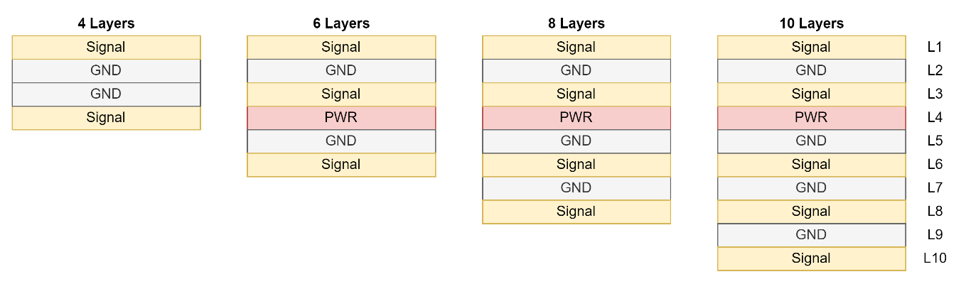
Finally, here are some of my favourite multilayer stackups that follow the guidelines we previously outlined.
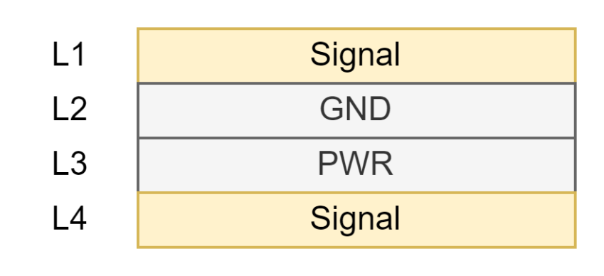
Four-layer (routed power): SIG – GND – GND – SIG
Six-layer: SIG – GND – SIG – PWR – GND – SIG
Eight-layer: SIG – GND – SIG – PWR – GND – SIG – GND – SIG
Rick Hartley Video
Lastly, I cannot recommend a video by Rick Hartley enough on how to achieve proper grounding and choose your layer stackups correctly. In the video, Rick talks about many of the principles outlined in this article in far more detail.
Whether you need to build reliable power electronics or advanced digital systems, use Altium’s complete set of PCB design features and world-class CAD tools. Altium Develop provides the world’s premier electronic product development platform, complete with the industry’s best PCB design tools and cross-disciplinary collaboration features for advanced design teams. Experience Altium Develop today!

About Author
Related Resources
Related Technical Documentation
Table of Contents
Design to Release, Without the Friction
- Keep reviews tied to the right version
- Reduce handoff confusion and rework
- Spot sourcing and release risk earlier
- Work solo, share when needed
Get Started
Thank you, you are now subscribed to updates.

