


How Reliable is Your Hybrid PCB Stackup?

At a Glance
Do you know whether your hybrid PCB stackup is reliable? What can your fabricator do to help ensure reliability? Read this article to learn more.


PCB stackups often incorporate slightly dissimilar materials that could pose a reliability problem. Hybrid PCBs are one case where the PCB stackup will include different materials, typically a standard FR4 laminate and a PTFE laminate for RF PCBs. While I was at PCB East last month, I received a question about the reliability of these stackups and what factors could influence reliability, quality, and yield during manufacturing.
After doing some digging, I decided to write this article and discuss some of the reliability challenges involved in designing high-quality PCB stackups with dissimilar materials. Designers who want to take the lead on material selection when designing their hybrid stackups should consider these factors that affect reliability. As with any PCB stackup, make sure you get your fabricator involved in the manufacturing process early to ensure reliability problems do not arise during production.
Risks of Hybrid PCB Stackups
If you’re unfamiliar with the basics of hybrid PCB stackups, including the benefits such layer stack structures may provide in terms of signal integrity, take a look at this article. The basic ideas involved in floorplanning an RF PCB with a hybrid stackup are detailed in the linked article. We often look at hybrid PCB stackups for RF systems, but they could really be used in any system where the low-loss layer(s) provide some benefit, including high speed digital systems.
With this in mind, there are some characteristics that create potential risks of using hybrid PCB stackups in some processes. Some characteristics to note include:
- Stackups may be slightly asymmetrical due to thickness differences
- Hole wall preparation for PTFE materials differs from that in FR4 materials
- Different laminates can have different CTE values, particularly when we compare PTFE and FR4 materials
- Required drill speeds will vary in different materials due to their mechanical strength
Take a look at the example stackup below. This is one of the hybrid stackup examples I like to show in high frequency PCB design courses.
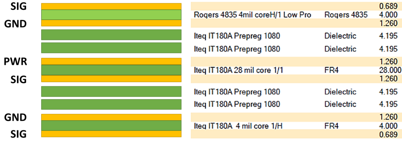
This is one instance where the design would best be used to support RF routing on only one layer. In addition, the internal layers are Iteq laminates with the bottom layer thickness matching the top layer thickness, so the stackup is symmetric. The only other deviation from the standard 6-layer PCB stackup is the use of stacked dielectric instead of cores between L2/L3 and L4/L5. This was enforced due to the RO4835 material being a core material.
Other hybrid PCB stackups may not implement the same symmetric type of stackup, although you should aim for this anyways. In the above stackup, and in other hybrid PCB stackups, we have some of the following reliability risks:
Hole Wall Plating Consistency
A PTFE layer used in a hybrid PCB stackup will use plasma etching to desmear drilled holes prior to plating. The process can have a higher etch rate on FR4 materials that might create an uneven surface. The hole wall would then need greater plating thickness to compensate. An allowance for up to 2x plating thickness in larger via holes is appropriate here to ensure consistent copper plating along hole walls.
Delamination
The major factor creating delamination risk is not the interlayer bond strength, it is the CTE value. CTE differences cause one material to expand faster than another, creating between the layers while the board is heated up to high temperatures. During extreme excursions (i.e., thermal shock or repeated extreme cycling), some delamination may occur in the stackup.
Deformation and Warping
According to Isola, the biggest challenge in fabricating a hybrid PCB layer stack involving PTFE is permanent deformation during thermal cycling (reflow and/or press-up), even if this does not result in delamination. This is another side effect of the higher CTE values in PTFE compared to FR4 materials (about 2x difference in the z-axis). Since process temperatures can reach 250 Celsius during manufacturing, the FR4 section will rise above its Tg value before the PTFE section, but the PTFE material layer will still exhibit a significant volumetric excursion that can result in permanent deformation.
Work With Your Fabricator Early
These factors can vary in prominence for different material pairs, and this is still an open area of investigation as more devices start incorporating low-loss materials with standard FR4 materials. As is the case with many designs that go beyond a simple FR4 stackup, working with your fabrication house early can help ensure success. If you plan to use a hybrid PCB stackup, you should make sure your fabricator has past experience processing these designs. Contacting them early to assess their experience and get their recommendations is the best path forward to ensure they know how to handle these reliability challenges.
My strategy for working with fabricators to engineer a hybrid stackup is to start with materials I’ve used before. I normally do this with Rogers materials, but you could work with others. I will then send the fab house a proposed stackup to see if they can hit my target layer arrangement. They will then send back a structure that they can do at the required layer count and dielectric/impedance data that incorporates the desired hybrid structure. From there, I can create the impedance design rules I need to layout and route the design.
If you want to make sure your hybrid PCB stackup will be reliable and have high yield, make sure you specify your fabrication requirements using Altium Designer®. After receiving your approved hybrid PCB stackup, you can enter your dielectric and impedance information using the Layer Stack Manager. Once you’ve created your PCB footprints and you want to share them with your collaborators, your team can work together through the Altium 365™ platform. Everything you need to design and produce advanced electronics can be found in one software package.
We have only scratched the surface of what is possible to do with Altium Designer on Altium 365. Start your free trial of Altium Designer + Altium 365 today.

About Author
Related Resources
Table of Contents
Design to Release, Without the Friction
- Keep reviews tied to the right version
- Reduce handoff confusion and rework
- Spot sourcing and release risk earlier
- Work solo, share when needed
Get Started
Thank you, you are now subscribed to updates.

