


What is PCB Routing?

At a Glance
Learn about PCB routing techniques and how to design traces to proper routing in any device. You can access the best PCB routing features in Altium Designer.


Routing PCB traces and vias on a PCB design is often thought of as a simple task. After importing the board and arranging components on the board, it would seem a relatively easy matter to start connecting components with copper. While that may have been true back in the days of low-speed TTL DIP components on simple boards, today’s design requirements are much more complex. Traces on a PCB can carry very specific design requirements that are meant to ensure signal integrity during routing.
Although traces might have specific routing requirements, today’s more advanced PCB routing techniques and features can help you set up and follow design rules for your traces. The important routing techniques you’ll use for your board depend on the signaling standard you’re working with and the required routing topology. If it’s your first time designing a PCB router and you’re ready for the routing phase, then don’t fret, we’ll show you how to route a PCB and determine the routing requirements you should follow in your PCB routing guidelines.
Starting PCB Routing
So what is PCB routing? All PCB routings need to have copper that connects components on the surface layer or internal layers, known as traces. What qualifies as a “simple” device depends on several factors, which will determine the appropriate trace design you use in your PCB. Some of the important design routing requirements you’ll find in low-speed and high-speed signaling standards include the following:
- The current carrying capacity of traces, as high current boards can require large traces or even polygons
- Trace width to be used in the board, which will ensure manufacturability and will affect crosstalk
- Any controlled impedance signals, which require specific width that must be set based on the PCB stack-up
- Routing PCB topology, which will determine how traces branch connect to multiple components
- Total losses along a trace, which determines the maximum allowed trace length
- Allowed skew in parallel buses and differential pair routing guidelines; protocols with source-synchronous clocks (SPI or I2C) and parallel buses all have maximum skew specifications
As a designer, your job is to find a balance in all of these areas and determine which of the points in the above list are most important for different nets. For example, high-speed designs rely on controlled impedance with differential pair routing guidelines, while high-current DC designs need to have wide traces that do not necessarily have specific impedance.
To get started, let’s look at some of the routing requirements for more basic boards, then we’ll jump into more advanced designs.
Simple PCB Trace Routing
If your design is not running at high speeds, it is not dense enough to create problems with crosstalk, and your traces need to carry low current, then you are typically free to select a trace width that easily accommodates your component pins and leads. Trace widths ranging from 5-15 mils can be used in these designs as they will be small enough to be routed directly into pads on most components. A basic example with an op-amp is shown below, where traces are being routed between a low-speed IC, some resistors, and capacitors.

Simpler designs like this generally aren’t concerned with impedance, standard routing topologies, or high currents. However, very few modern designs are so simple that they don’t require some level of trace design or determination of routing rules.
Routing Rules for Modern PCBs
Today’s boards, even those that only use a simple MCU and low-power stages, require some level of trace design and routing rules to ensure signal integrity. Designers need to determine the trace geometry requirements for their connections to ensure reliability and signal integrity.
- Determine the current requirements in a given trace; routing PCB power circuits can carry high currents.
- If the current will is very low (less than 1 A), determine whether impedance control is needed by looking in your component datasheets or your signaling standard.
- Calculate the trace width needed to hit your impedance target if impedance control is needed. Also, calculate the trace spacing needed if differential pair routing guidelines are needed.
If impedance control is needed, it’s likely a routing topology will be implemented with single-ended or differential pair routing rules. Be sure to check your signaling standards to determine your routing requirements, which will include things like loss budget (determines total length), impedance requirements, and allowed length mismatch in differential pairs or in a parallel bus.
- Learn more about designing traces for impedance-controlled routing
- Learn more about trace design for high-current PCBs
Once you’ve determined any routing requirements in your board, you can set up design rules for specific nets in your design. This involves setting minimum or maximum trace widths in your design rules, and your routing tools will use these specifications to set the trace width as you route traces.
Impedance and Routing Topology
When you need impedance control in your PCB layout, you’ll need to determine the impedance using one of several methods. There are formulas you can use to determine the impedance in your design, or you can use more specialized applications to calculate the impedance you need in your design. Single-ended and differential pair routing guidelines impedance will have defined geometry to ensure impedance goals are met.
- Learn more about determining microstrip trace impedance
- Learn more about determining symmetric stripline trace impedance
The fastest way to determine impedance is in PCB design software that includes a built-in calculator tool. Not all PCB design applications will include this type of utility, and those that do produce results with differing levels of accuracy. The best PCB design applications will include an electromagnetic field solver that automatically calculates the required trace geometry. These tools will take the dielectric constant and copper roughness information in your PCB and use it to calculate the trace width and differential pair spacing needed to hit a target impedance.

Trace routing topologies define how traces are routed between component inputs and outputs, as well as how traces are branched from each other to reach multiple components. For example, DDR routing uses a fly-by topology, where a single bus branch off to reach multiple components in the design. In another example, SPI uses a similar bus topology, but with termination applied near the driver on the bus. Other components might use point-to-point topology to reach multiple components, which is most common when a design requires a single component to communicate with multiple loads over a single IO interface. Make sure you understand the routing topology needed in your signaling standards, as well as whether those traces require impedance control.
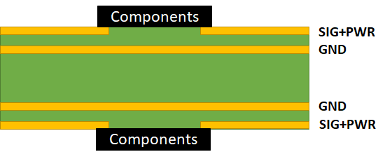
Routing on Multiple Layers
The simple examples shown above illustrate PCB routing on a single layer. In reality, most commercial boards involve multiple layers of routing, even if it is only the two surface layers. More advanced boards can involve 4 layers at minimum, where routing is typically on the surface layers and the internal layers are planes (ground).
The basic 4-layer stackup that provides routing on multiple layers is shown in the example image below. Once your stackup reaches at least 6 layers, you can have at least one internal layer for routing signals.
- Learn more about basic 4-layer stackups
- Learn more about 6-layer and higher stackup designs that enable multilayer routing
In order to route on the back layer, signals need to transition across the layer stack using vias. Multilayer routing in digital boards with vias requires ensuring two important design features are implemented during routing:
- The signal layers are routed over ground pour or complete ground planes
- The ground regions under the signal layers are also connected together with vias
One strategy that is often used on 2-layer boards is to use orthogonal routing, where traces are routed in perpendicular directions. This gives a simple way to route across two different layers in two different directions. An example is shown in the image below.
In this strategy, the top layer (red traces) is used only for horizontal routes. In order to complete a route that requires a vertical section, a via is used and the vertical section is placed on the bottom layer (blue traces). This strategy helps simplify routing, especially in boards with many parallel buses and high GPIO counts.

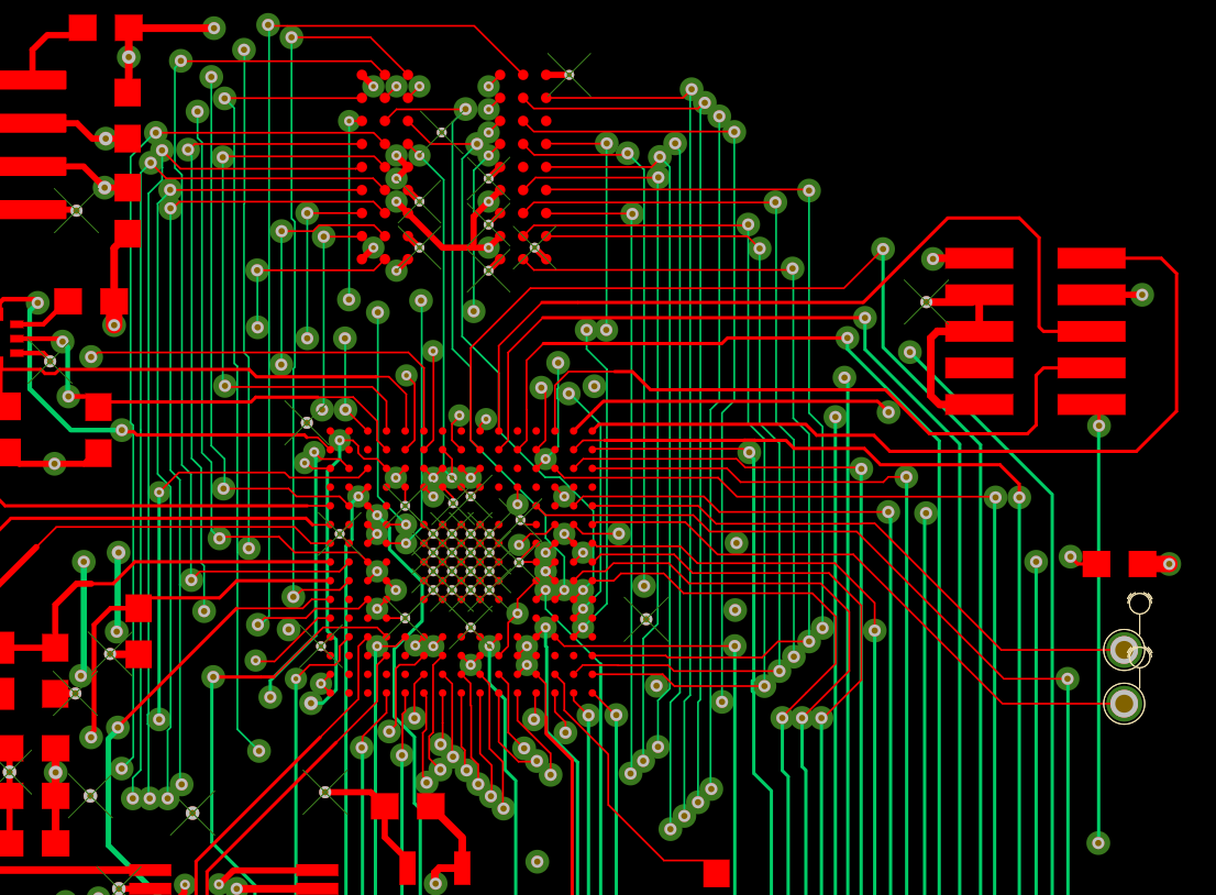
A more advanced example involving orthogonal routing with many traces and components is shown in the image below. In this example, an MCU is used as the main processor and its I/Os are being routed to multiple ASICs. Some of these traces are impedance controlled to 50 Ohms, which are being used to route into a RAM chip in the top half of the layout image. Just as was the case in the above example, the orthogonal routing implemented here is being used to enforce vertical and horizontal routes on different layers. The example below uses a 6-layer stackup with routing on an internal layer.
Basic Guidelines for Signal Integrity
Signal integrity is one area that is intimately related to PCB stack-up design and routing. The arrangement of plane/GND/PWR layers with respect to your signal layers and routing is a major determinant of signal integrity, and routing over complete sections of GND is the best way to ensure your design will maintain signal integrity and have immunity to EMI (crosstalk, external RF noise, power supply noise, etc.). This simple guideline and the routing rules shown above will help prevent or reduce many signal integrity problems and will help ensure your board remains functional.
Some important PCB routing guidelines you should consider include:
- Try to keep controlled impedance traces for a given interface or signaling protocol on the same layer
- Minimize via transitions on high-speed protocols and RF traces
- Be careful not to route over splits in planes and keep track of the return path in your PCB; the best way to do this is to use uniform ground regions
- Try to keep traces short and direct, don’t make traces longer than they need to be
- For high current routing, don’t be afraid to use polygons to construct larger conductors; these can be used to make any shape conductor
Before you start routing PCB traces, take some time to develop a strategy for different routes to ensure you don’t make excessive use of vias or need to add additional layers to solve the board. Your PCB routing strategy will depend on your PCB layout; if too many nets are crossing in the PCB layout, you’ll have a more difficult time routing traces without excessive layer transitions. At times, you’ll have to start with the easiest routes first as these will help you pin down which routes take more time and effort to fully route in the PCB layout.

The most advanced routing tools that can help you stay in line with basic PCB routing guidelines are interactive. In other words, these tools are semi-automated, allowing you to define routes for a group of signals, and the routing tools will place traces such that they automatically obey your design rules. In this type of routing, the design rules for your nets and groups of nets are checked automatically as you create your PCB router layout. Many freeware and open-source design programs force you to do everything manually, but advanced PCB design programs like Altium Designer can help you stay productive as you work to complete your PCB router layout and route traces around your board.

PCB routing techniques is much easier when you use the complete set of PCB layout tools in Altium Designer®. The integrated design rules engine in Altium Designer automatically checks your routing as you place traces, allowing you to spot and eliminate errors before you finish the board. Every Altium Designer user also has access to a dedicated workspace in the Altium 365™ cloud platform, where projects, component data, manufacturing data, and any other project documentation can be stored and shared with collaborators.
We have only scratched the surface of what’s possible with Altium Designer on Altium 365. If you want to learn more about what is PCB routing you can start your free trial of Altium Designer + Altium 365 today.

About Author
Related Resources
Related Technical Documentation
Table of Contents
Design to Release, Without the Friction
- Keep reviews tied to the right version
- Reduce handoff confusion and rework
- Spot sourcing and release risk earlier
- Work solo, share when needed
Get Started
Thank you, you are now subscribed to updates.

