


PCB Routing Rules For Differential Pairs and Single-Ended Signals

At a Glance
Different signaling standards require different PCB routing rules. Here’s how to find and set the PCB routing rules you need in your PCB design software.


Sometimes, the distinction between what qualifies as a “slow” or “fast” signal can seem arbitrary, and it might depend on who you ask. A related topic is whether a PCB trace is considered electrically “short” or “long,” and you might find just as much disagreement on the topic. Whether you need to route slow or fast signals in your PCB, your traces will need to follow some PCB routing rules to ensure your board functions as intended.
Like many other programs, Altium Designer included in Altium Develop helps make this process easy, but also goes a bit further and separates PCB routing rules for slow and fast signals into their own categories. Before you start routing signals between components, you’ll need to take a look at your design rules and adjust them to your signaling standards. Here are the important PCB routing rules you need to set before you start routing signals around your PCB.
PCB Routing Rules for Single-Ended Signals
Perhaps the most important point to note about PCB routing rules is that routing standards do not necessarily define themselves as “low speed” or “high speed.” This distinction has been largely created and perpetuated by PCB designers, and it largely arose due to signal integrity problems that arise when signal rise times become very fast (less than ~1 ns). As such, it’s more important to understand the constraints in your signaling standards when setting up your design rules, regardless of whether you’re dealing with slow or fast signal speeds.
The first place to look for the design rules you need is in the documentation for your signaling standards. The documentation for most standards is freely available online. As you create more designs, you’ll become more familiar with these standards and you’ll know which rules to set in your designs. Some of the most common PCB routing rules that apply to many standards for single-ended signals are:
- Matched lengths. For bus standards or parallel data routing with source-synchronous clocking, you’ll need to enforce length matching for all nets in a group within some tolerance. While routing, this is done by adding length tuning structures to a net.
- Via transitions. Some standards recommend limiting the number of via transitions to prevent excess loss, reflections, and other parasitic effects.
- Maximum length. The maximum length of a net is sometimes specified for a given loss tangent value to prevent excessive signal attenuation. If you’re using a low-loss laminate, you can extend the length depending on the difference in loss tangent values.
- Clearances. Traces need to be kept separated from other objects that aren’t part of the net (pads, components, planes, etc.). This ensures manufacturability, reduces unwanted parasitics, and provides ESD protection in high voltage design.
- Width and impedance. These two quantities are interrelated and are used for controlled impedance in high speed design. Take a look at this article to see how you can specify impedance and trace width as PCB routing rules.
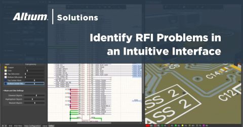
All these design rules and many more can be accessed in the PCB Rules and Constraints Editor in Altium Designer. If you need to assign the same PCB routing rules to a group of nets (very common for groups of single-ended signals), the quickest way is to assign all nets in a group to a Net Class. You can access this feature from the Design → Classes option (see below) in the PCB Editor window. After you’ve assigned nets to classes, can then use the PCB Rules and Constraints Editor to assign design rules to individual nets or to a Net Class.

Other PCB routing rules that may not apply to specific signaling standards are used to help ensure you keep your design organized. Two prime examples are routing topology and routing layer restriction. For more advanced designs, such as components with BGA footprint, you can use design rules to configure your fanout strategy. Working with differential pairs requires its own set of design rules, as shown in the next section.
Differential Pair Routing Rules
Differential pairs are unique because slow and fast signals can be routed as differential pairs. Regardless of whether the signals are fast or slow, your differential pairs still need to obey some design rules that you would normally enforce for single-ended signals. Four important design rules to consider for differential pairs are:
- Impedance tolerance. Even if you’re routing at less than the critical length, it’s best to bite the bullet and create an impedance profile for your differential pairs unless your signaling standard says otherwise. Other geometry constraints will depend on the allowed impedance variation along the differential pair.
- Maximum uncoupled length. This tells you the longest distance that the two sides of a differential pair can remain uncoupled (i.e., separated by a large distance). This is important as the uncoupled section will look like an impedance discontinuity, so it must be sufficiently short.
- Length matching. Remember, a differential signal is read by taking the difference between the two signals, so the two signals need to arrive at the receiver simultaneously. Faster signals require smaller length matching tolerances.
- Maximum net length. Just like single-ended signals, differential signaling standards may have a maximum length constraint. Consider CAN bus as an example; even though this is a slow-speed standard, the maximum link length (PCB traces + cable) will depend on the data rate you’ll use in your system.
In Altium Designer, you can set up design rules for the first two points above in the Routing → Differential Pairs Routing area of the PCB Rules and Constraints Editor. The other two points can be addressed in the High Speed area. This is shown for the image below:

If you’re working with high speed differential pairs, any of the other standard high speed design rules discussed above can be applied to differential pairs. Note that the easiest way to do this is to assign the relevant differential pairs to a Differential Pair Class, and then select the class that will be governed by each design rule.
If a design rule is not configured to accept a Differential Pair Class in the “Where The Object Matches” drop-down menu, you can create a Custom Query using the query builder. This is shown below for assigning maximum length to a Differential Pair Class (found in the High Speed area of the PCB Rules and Constraints Editor).

Just like with single ended nets, read the documentation on your signaling standard before you start setting PCB routing rules. This is where you’ll find the relevant design rule information for differential signaling standards (usually in the Physical Layer section of the standard). Take a look at this article to see how to create an impedance profile, assign nets to Differential Pair Classes, and set up some design rules for these classes before you start routing differential pairs.
We still haven’t looked at signal integrity rules for fast signals, and by now you’ve probably noticed that Altium Designer includes design constraints specifically to address signal integrity problems. You can assign these PCB routing rules with the same process you followed for adding design rules to single-ended nets and differential pairs. These features in Altium Designer give you full control over your design and help you route successfully.
What Values Should You Use For Design Rules?
This is always a tough question to answer because it depends on many factors. Most importantly, it depends on the interface you are using; USB will have different constraints than PCIe, for example.
Assuming you have the specification for your interface and signals, you can quickly derive some design rule constraints and limits, either from calculating by hand or through some worst-case estimation.
|
Trace width (single-ended) |
Based only on impedance target |
|
Trace width and spacing (differential) |
Based on differential impedance target and odd-mode impedance deviation |
|
Trace-to-trace spacing (crosstalk) |
|
|
Length tuning limit |
Determine based on
|
|
Trace length |
Based on total insertion loss, can be calculated from: |
For some of these values, such as insertion loss, you might have to use an external transmission line simulator to get an accurate loss value, or you will have to estimate the value from some calculations. For other design rules, such as mode conversion, simulation could happen after routing is complete in order to diagnose whether there are problems in the routing.
Altium Designer within Altium Develop delivers an unprecedented amount of integration to the electronics industry until now relegated to the world of software development, allowing designers to work from home and reach unprecedented levels of efficiency.
Whether you need to build reliable power electronics or advanced digital systems, Altium Develop unites every discipline into one collaborative force. Free from silos. Free from limits. It’s where engineers, designers, and innovators work together as one to create without constraints. Experience Altium Develop today!

About Author
Related Resources
Related Technical Documentation
Table of Contents
Design to Release, Without the Friction
- Keep reviews tied to the right version
- Reduce handoff confusion and rework
- Spot sourcing and release risk earlier
- Work solo, share when needed
Get Started
Thank you, you are now subscribed to updates.