Increase Component Density in Multilayer PCB Design with Blind Vias
As component density increases, the via strategy usually changes before anything else. Designers can keep shrinking placement spacing and pushing routing into inner layers for a while, but eventually conventional through-hole vias start consuming too much surface area and too many routing channels. That is the point where blind vias start to matter. They are one of several interconnect structures used when package pitch, fanout routing clearance, and layer usage begin to exceed what a conventional via field can support.
The real question is when to use blind vias in a PCB, and when the design has moved into microvia, buildup, or via-in-pad territory. That decision is tied to fanout geometry, stackup construction, fabrication capability, and assembly consequences. If the design is dense enough that blind vias are on the table, then the rest of the HDI strategy needs to be considered at the same time.
Routing Density and Fanout Constraints
The first pressure point is usually fanout, not board outline. Fine-pitch BGAs, denser component placement, and double-sided assembly all compress the routing channels that would normally be available for escape routing. Through-hole vias become a problem because they block routing on every traversed layer, including layers that might otherwise remain available for signal breakout or power distribution. In moderate-density designs, that penalty is acceptable. In denser layouts, it becomes the dominant interconnect constraint.
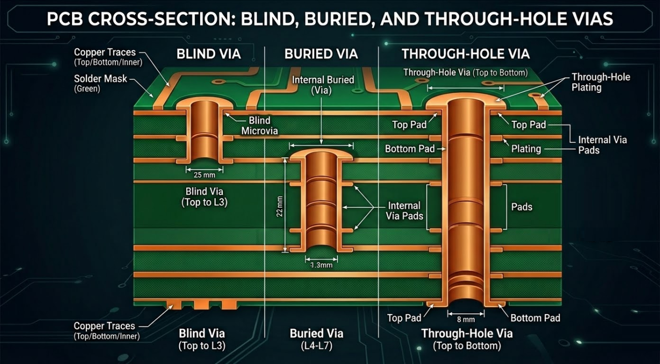
Blind vias solve part of that problem by terminating at an internal layer. That preserves area on the opposite side of the board for dense component placement and opens more routing channels in internal layers. For many multilayer boards, especially designs with dense BGA regions but not full HDI construction, this is the first step beyond standard plated through-holes.
Blind vias are usually the right next step when a design shows a few specific conditions:
- The outer layers no longer have enough routing channels for package escape.
- Through-hole vias are blocking too many inner-layer routes in dense component regions.
- The design needs more breakout flexibility under BGAs without committing immediately to full HDI construction.
- High trace density in specific package areas rather than spread across the entire board.
The limitation is that blind vias do not solve every density problem by themselves. As pitch decreases, the capture pad diameter, pad-to-pad spacing, and available breakout geometry can get tight enough that even a mechanically drilled blind via is still too large. At that point, the design stops being a generic blind-via board and becomes an HDI stackup problem.
The table below outlines the important case of via selection for BGA footprints, which are the most common component driving the implementation of blind vias.
|
1.0mm to 0.8mm pitch |
0.8 to 0.65 mm pitch |
Less than 0.65mm pitch |
|
|
|
From Through-Holes to Blind Vias and Microvias
It helps to evaluate the interconnect options in the order they would be considered during layout planning. Through-hole vias remain the lowest-complexity option and they are still the best choice whenever routing density allows them. They are cheaper, easier to fabricate, and less sensitive to aspect-ratio and filling constraints. The mistake is trying to keep them in a design after the geometry has already ruled them out.
Blind vias: Use when outer-layer routing area becomes too constrained and the board needs access from the surface into internal layers without giving up routing space on the far side of the board. They are useful when the density increase is real but not severe enough to force full HDI construction. This is common in multilayer digital boards with overlapping leadless parts (like BGAs), and high density of SMD parts.
Microvias: become relevant when pad diameters and spacing shrink further. At that point, the problem is not just getting to an inner layer. The problem is doing so with a small enough drilled structure and capture geometry that the fanout actually fits between pads and inside the escape region. Microvias also create shorter vertical transitions and can be arranged across buildup layers as staggered or stacked structures when multiple sequential lamination cycles are used.
|
Via structure |
Typical drill hole diameter |
Typical via aspect ratio |
Stacking and via-in-pad options |
|
Through-hole via |
As low as 6 mil but limited by board thickness |
Highest aspect ratio because the via spans the full board thickness |
- Stacking: No - Via-in-pad: Sometimes, but usually avoided unless specially processed |
|
Mechanical blind via |
Smaller than full through-hole vias, limited by mechanical drilling depth |
Can be same as through-holes, but typically lower (<10:1) |
- Stacking: No, not in the HDI microvia sense - Via-in-pad: Sometimes, depending on pad size |
|
Blind microvia |
Smallest drill diameter, as low as 2 mil with advanced processing |
<1 for reliable microvias |
- Stacking: Yes - Via-in-pad: Yes |
A practical selection process usually follows this order:
- Start with through-hole vias unless fanout geometry clearly rules them out
- Move to either via-in-pad or blind vias (or both) when outer-layer density is the main problem
- Move to blind microvias when capture-pad size and fanout routing clearance become the major constraint
- Clearly specify the via type when via-in-pad is used on mechanical drills
Via-in-pad is a more selective tool. It is useful when the package geometry leaves no room to place a via outside the pad, or when routing has to leave the pad directly to reach an internal layer. Fine-pitch BGAs are the obvious example, but the same logic can apply to LGAs, QFNs, and exposed-pad packages.
Microvia Aspect Ratio and HDI Stackup Limits
Microvias are often described as simply small vias, which is not a very useful engineering description. The real constraint is aspect ratio (via depth to via diameter ratio). Once the depth becomes too large relative to the drilled diameter, plating quality, filling quality, and long-term reliability all become harder to control. That is why microvia decisions have to start in the stackup. You do not choose the hole size in isolation and then hope the buildup structure will support it.
The outer dielectric thickness and copper thickness both matter because they define the total depth that the laser-drilled structure has to span. If the buildup layer is too thick, the microvia diameter has to increase, which then consumes more pad area and starts to defeat the routing benefit. This is one reason HDI stackups are built around thin outer dielectric layers and sequential buildup structures rather than treating microvias as direct replacements for conventional drilled vias.
A practical design review should confirm a few points before fanout rules are finalized:
- Whether package pitch supports conventional fanout, blind-via fanout, or requires microvia fanout
- Whether buildup thickness supports the intended microvia diameter and aspect ratio
- Whether the fabricator allows the required fill process, stacking approach, and pad structure
- Whether advanced via structures can be limited to localized high-density regions instead of the full board
Fabrication and Assembly Consequences
Once the interconnect structure gets denser, the board stops being just a routing problem and starts becoming a fabrication and assembly problem. Mechanically-drilled blind vias add process complexity and copper weight on any layer where they terminate, which will change the allowed feature sizes in the design. If you add microvias instead, you now have tighter process limits on drilling, plating, and filling; reliability testing may also reveal limitations on the allowed number of HDI build-up film layers, regardless of stacking.
If your placement reveals the need for blind vias (whether mechanical-drilled or laser-drilled), ask your fabrication house for their capabilities before defining via sizes and linewidth/spacing rules.
Whether you need to build reliable power electronics or advanced digital systems, use Altium’s complete set of PCB design features and world-class CAD tools. Altium provides the world’s premier electronic product development platform, complete with the industry’s best PCB design tools and cross-disciplinary collaboration features for advanced design teams. Contact an expert at Altium today!
Frequently Asked Questions
Do most PCB fabrication companies support blind vias?
Yes. Most PCB fabrication companies can accommodate blind via designs. The ability to drill and plate blind vias is a standard capability, whether using mechanical drilling or laser drilling for microvias. This is the case in the United States, China, and Europe.
Are special PCB manufacturing outputs needed to specify blind vias?
Typically, a designer should output one drill table and NC drill file for each via span. So for example, if you have two blind via spans and through-holes, you would output 3 NC drill files and include 3 drill tables in your fabrication drawing.
Can I use blind vias with via-in-pad?
Yes. You can use via-in-pad with any type of via, including mechanically drilled blind vias and laser drilled blind microvias. Blind microvias will require full plating to fill the via so that it fully closes when used in a via-in-pad design.
Are blind vias reliable?
Mechanically-drilled and laser-drilled blind vias are widely viewed as reliable as long as they are built within aspect ratio and annular ring constraints. When used in leadless parts like QFNs or BGAs, these vias tend to be very small and may experience reliability problems under thermal cycling, particularly for blind microvias used in via-in-pad structures. Design teams should do their own reliability assessments for their products in the field before allowing blind vias in manufactured products.
Does Altium support blind via usage?
Yes. Altium allows users to use blind vias as a standard feature. If using blind vias in a via-in-pad configuration, make sure to enable the “Vias Under SMD” rule in the PCB Rules and Constraints Editor. Read the Altium Designer Documentation to learn more.

