


I/O Expansion For Digital, Analog, and Mixed Signals

At a Glance
See how I/O expansion works for digital signals, analog signals, and mixed-signal interfaces.


It's often the case that a single I/O needs to be received by multiple loads, whether it's in the analog or digital domain. In many systems, a microcontroller or processor has a limited number of available pins, yet the design requires driving or sensing signals across a larger number of endpoints. This creates a fundamental routing and architecture problem that must be solved at the board level, and the solution depends heavily on whether the signals in question are digital, analog, or a combination of both.
The methods for expanding I/O capacity differ substantially across these domains. Digital expansion is well-served by dedicated protocol-based expander ICs, while analog fanout requires active buffering or multiplexing to preserve signal integrity. Mixed-signal interfaces present the most constrained design problem because they demand both digital control logic and analog signal conditioning in a compact implementation. Understanding the tradeoffs in each domain helps designers select the right architecture without over-engineering the solution or sacrificing performance where it matters.
Digital Signal I/O Expansion
The primary method for expanding digital I/Os is through a dedicated ASIC that supports the communication protocol used by the host controller. These expander ICs accept commands over a serial bus and present additional general-purpose I/Os to the system without consuming large numbers of processor pins. Common protocols supported by digital I/O expanders include:
- I2C
- SPI
- SMBus
- Custom GPIO-based interfaces
When selecting a digital I/O expander, designers should evaluate whether level shifting is required between the host bus voltage and the expanded output voltage domain. Many modern I/O expanders incorporate level-shifting capability on-chip, eliminating the need for external translators. However, if the expander does not support the target logic levels natively, external level shifters must be added, which increases board area and component count. Drive strength, output type (push-pull versus open-drain), and interrupt capability are additional selection criteria that affect how cleanly the expander integrates into the broader system architecture.
Analog Signal Fanout
Analog signal fanout distributes a single source signal to multiple independent loads using active buffering. Unity-gain op-amp followers present high impedance to the source while providing low-impedance copies at each output, preventing loading effects and isolating downstream channels from one another. For higher channel counts, dedicated analog mux/demux ICs or crosspoint switch matrices provide structured routing under digital control, though they introduce on-resistance, charge injection, and bandwidth constraints that must be evaluated against the application requirements.
In applications requiring signal conditioning during fanout, instrumentation amplifiers or programmable gain amplifiers can be placed at each output stage to provide gain, filtering, or impedance matching tailored to each load. The choice between passive distribution, active buffering, and switched routing depends on the required bandwidth, channel isolation, and whether simultaneous or time-multiplexed output is acceptable. The table below summarizes the primary tradeoffs across common fanout architectures.
| Fanout Method | Simultaneous Outputs | Bandwidth | Channel Isolation | Key Limitation |
|---|---|---|---|---|
| Unity-gain op-amp buffers | Yes | High (GBW-limited) | High | Component count scales with outputs |
| Analog mux/demux | No (time-multiplexed) | Moderate | Moderate | On-resistance, charge injection |
| Crosspoint switch matrix | Yes (configurable) | Moderate | Moderate-High | Package size, cost at high channel count |
| Resistive distribution | Yes | High | Low | Signal attenuation, load interaction |
Some additional design considerations for analog fanout circuits include:
- Source impedance must remain low relative to the parallel input impedance of all buffer stages to avoid gain error at the distribution node.
- Each buffer output should be decoupled from shared power rails to prevent crosstalk through supply-induced coupling.
- If there is phase/timing sensitivity, trace routing from the distribution node to each buffer should be length-matched.
Compact Mixed-Signal I/O Expansion
Programmable mixed-signal processors integrate configurable analog blocks (comparators, amplifiers, DACs, voltage references) alongside digital logic elements (look-up tables, flip-flops, counters, delay blocks) within a single IC. The result is effectively a CPLD-equivalent for analog signals: designers implement a custom analog front-end inside the chip itself, configured through software rather than built from discrete op-amps, comparators, and passive networks spread across the board.
This architecture eliminates discrete analog circuitry, reducing component count and shrinking board footprint significantly compared to equivalent discrete solutions. It also removes many layout sensitivities associated with high-impedance analog nodes routed across a PCB. Programmability means the same physical device can be reconfigured for different analog interface requirements without a board respin, and combining digital control logic with analog signal processing in one package simplifies partitioning between analog and digital domains.
GreenPAK as a Mixed-Signal I/O Platform
GreenPAK from Renesas is a family of non-volatile memory configurable mixed-signal ICs that integrate analog blocks (op-amps, comparators, voltage references, ADCs) with digital logic (LUTs, flip-flops, counters, delay elements) in a single small-footprint package. These devices are programmed through a graphical schematic-based tool rather than HDL, making them accessible for hardware engineers building custom interface logic without traditional FPGA workflows.
Designers can build and simulate a mixed-signal interface expander with an integrated analog front-end for a GreenPAK component using the Go Configure software from Renesas. The tool provides a drag-and-drop design environment where internal analog and digital resources are connected visually, simulated for functional verification, and then programmed into the target device through a development kit.
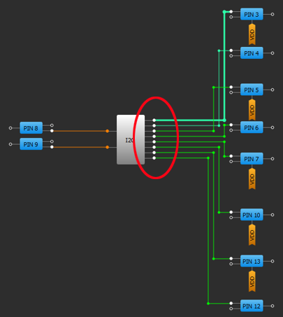
GreenPAK I/O expander design in the Go Configure software.
To learn more, take a look at the GreenPAK components and reference examples.
Whether you need to build reliable power electronics or advanced digital systems, use the complete set of PCB design features and world-class CAD tools offered by Altium to implement your GreenPAK solutions. Altium provides the world’s premier electronic product development platform, complete with the industry’s best PCB design tools and cross-disciplinary collaboration features for advanced design teams. Contact an expert at Altium today!
Related Resources
Related Technical Documentation
Table of Contents
Design to Release, Without the Friction
- Keep reviews tied to the right version
- Reduce handoff confusion and rework
- Spot sourcing and release risk earlier
- Work solo, share when needed
Get Started
Thank you, you are now subscribed to updates.

