


Making Mixed-Signal Level Shifting More Compact

At a Glance
Level shifting is normally dedicated for digital signals with dedicated ICs, but there is no solution for analog or mixed-signal interfaces. GreenPAK offers a highly integrated solution for this application.


Voltage translation is normally framed as a purely digital problem. For example, a 1.8V device needs to talk to a 3.3V device, and the 3.3V device needs to interact with another device at 5V, and so on. In these cases, we normally check that an input can handle an expected signal level, and we might adjust the level with resistors or a dedicated level shifter IC. In the case of digital data, such as an I2C or SPI interface, a level shifter IC rated to the particular specification is most common.
In our experience, level shifting happens much more often in analog systems rather than digital systems, and yet there are no compact solutions for implementing analog level shifting in a PCB. However, analog shifting is still important for the same reasons as in digital designs, and it places more effort on circuit designers to devise circuit-based solutions for level shifting. There are ways to make this more compact for analog and mixed-signal systems, which we will discuss in this article.
Digital Level Shifters
Level shifting with digital signals can be performed by building a circuit from discrete components, but due to the speed and complexity of such circuits, it makes more sense to use a level shifter IC. These components provide direct level shifting between two voltages for digital signals, with voltages provided by separate power supplies. These components are common among semiconductor manufacturers, and although differing in specifications, they may have common pinouts and packages.
Some important electrical specifications of level shifters include:
- Supported interfaces (I2C, SPI, etc.)
- Output slew rate and clock frequency/data rate limit
- Directionality (uni-directional vs. bi-directional)
- ON-state resistance
- Additional integrated features, such as circuit protection or configurable slew rate
Typically these support single-ended interfaces, which may be standardized or simple GPIO level shifting as either open-drain or push-pull. In addition, some components may support very large input voltage ranges on one side of the shifter. For example, Renesas part number RH4Z2501 also functions as a line driver and can support input voltages up to 36V.
In bi-directional level shifters, the pad arrangements are often placed on each side of the component package. An example for Texas Instruments part number TXV0108 (proprietary RGY package option) is shown below. This pin arrangement makes fan-in and fan-out much simpler.
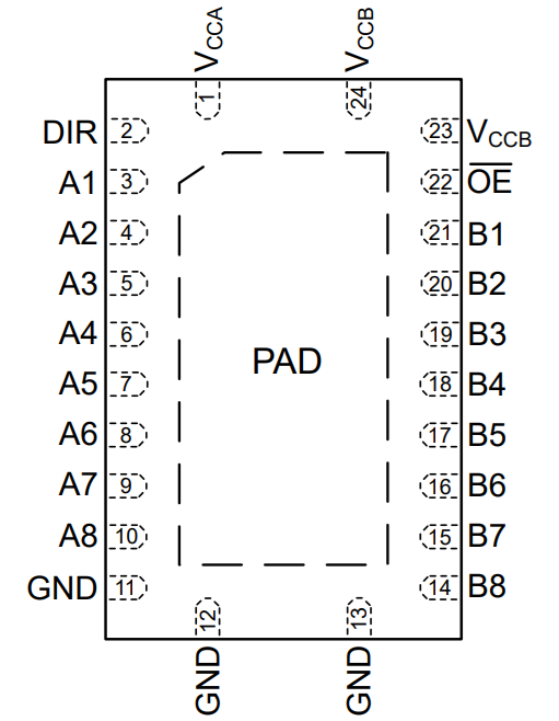
Pad arrangements on digital level shifters allow direct input/output routing on each side of the component in a PCB layout.
Analog Level Shifting Circuits
Analog level shifting involves adjusting the level of an analog signal by applying a DC offset, increasing/decreasing the analog signal peak voltage, or both. This is normally accomplished with custom circuitry, typically built with op-amps, and it is common to apply some additional filtering in the process of level shifting for purposes of noise cleanup.
Depending on which engineer you ask, you’ll find multiple ways to achieve the same type and magnitude of level shifting applied to an analog signal, each of them dedicated to a different type of signal or frequency range (or both). In fact, this is probably the reason dedicated analog level shifters with specific topology have never been built as ICs. That being said, we have seen several interesting methods for implementing level shifting with analog signals:
- Op-amp based solutions
- ADC-MCU-DAC signal chain designs
- Op-amp + ADC/DAC solutions
- Resistor divider-based circuits (for step-down)
- Bi-directional buffer solutions
This is just a small selection of the possible approaches for level shifting with analog signals. With so many options available, it should be clear why integrated solutions are hard to find. This is where a mixed-signal processor can provide value as an integrated solution for analog level shifting.
Mixed-Signal Level Shifting in GreenPAK
Clearly there are plenty of solutions for digital designs, and it is possible to build level shifting solutions for analog designs, but what about mixed-signal interfaces? These components would need to be custom-designed in silicon, and that is exactly what is possible with a programmable mixed-signal processor like GreenPAK.
In a GreenPAK component, a designer can configure mixed-signal macrocells for level shifting of digital and analog signals simultaneously, even in an asynchronous manner. GreenPAK devices allow simultaneous level shifting of multiple signals with additional logic processing implemented in the device as needed. This means a designer can accommodate standard digital interfaces, custom logic, or both alongside level shifting for analog signals.
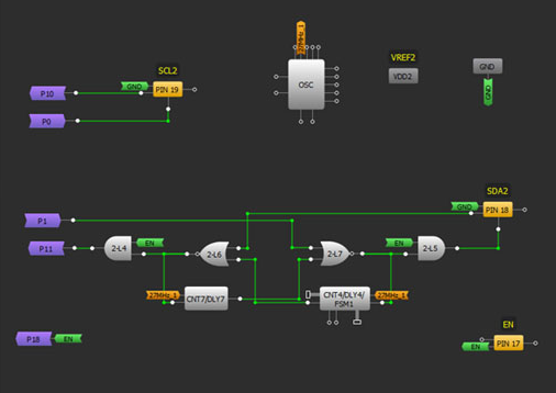
Graphical programming of a GreenPAK component.
The developer tools in Renesas GreenPAK give designers the ability to develop fully custom digital, analog, or mixed signal ICs that provide a dedicated level shifting function, or level shifting as a built-in feature. These programmable mixed-signal processors allow consolidation of additional logic functions instantiated directly in silicon, allowing for smaller, more efficient systems.
To learn more, take a look at the GreenPAK components and reference examples.
Whether you need to build reliable power electronics or advanced digital systems, use the complete set of PCB design features and world-class CAD tools offered by Altium to implement your GreenPAK solutions. Altium provides the world’s premier electronic product development platform, complete with the industry’s best PCB design tools and cross-disciplinary collaboration features for advanced design teams. Contact an expert at Altium today!
Related Resources
Related Technical Documentation
Table of Contents
Design to Release, Without the Friction
- Keep reviews tied to the right version
- Reduce handoff confusion and rework
- Spot sourcing and release risk earlier
- Work solo, share when needed
Get Started
Thank you, you are now subscribed to updates.

