


Layer Stackup in Flex and Rigid-Flex PCBs

At a Glance
Learn about everything that goes into designing flex and rigid Flex PCB layer stacks.


Layer stacks for flex and rigid-flex PCBs follow different rules from the standard rigid stack-up design process. Rigid designs use cores and pre-pregs to form layer stack-ups, while flex and rigid-flex designs use sheets of polyimide and adhesives to build up the layers. With a basic understanding of these materials, you can build high-quality flex layer stacks, including complex bifurcated flex designs and rigid-flex designs.
Here we can examine 3 types of designs involving flexible materials:
- Fully flexible PCB
- Flexible PCB + stiffeners
- Rigid-flex PCB
Each of these types of flex/rigid-flex designs has different layer ordering requirements and asymmetry allowances, which ultimately will impact where components can be placed and how the design functions. Let’s examine each of these types of flex designs.
Material Ordering in Flex Stackups
I like to start flex and rigid-flex designs with the central flex layer and then build outward. The simplest central layer arrangement includes pieces of the polyimide core, adhesive, and laminated copper. If the design is only two layers, then the copper is coated with a coverlay adhesive layer. For more than two layers, we can laminate more sheets of copper-coated polyimide together using an adhesive and insulating polyimide.

Additional layers are laminated onto the flex core using an adhesive and polyimide. This creates the repeatable pattern shown in the above stackup image. This allows the polyimide stack to continue building up to higher layer counts as needed.
Rigid Material Integration
This covers the basic layer arrangement for polyimide materials, which make up the flexible stack-up or the flex section of a rigid-flex design. Once we integrate rigid materials, we have additional material considerations. Rigid materials can be used in two ways:
- As stiffeners, only providing structural support but not used for routing
- As part of the layer stack, providing copper layers stacked onto the flexible core
Unlike conventional rigid PCB stack-ups, flex PCBs with stiffeners and rigid-flex PCB stack-ups do not have standard thicknesses. When a stiffener is applied, it can be any thickness as long as it can be reliably processed onto the flex layer arrangement. When a rigid-flex PCB stack-up is used, we do not build up the entire rigid plus flex stack into a standard thickness. Technically, any number of layers could be used and the arrangement does not need to be symmetric above and below the flex region.
Flex PCB + Stiffeners
Stiffeners are most commonly a single ply of FR4 prepreg bonded to the flex layer with adhesive. Note that other materials can be used as a stiffener, including a metal backing, advanced polyimide, or PTFE (normally a bondply). Once heated and pressed, the prepreg and the adhesive will bond together, and processing can continue for the rigid portion of the design. The coverlay extends up to the edge of the stiffener as follows:

Finally, the stiffener will not have any laminated copper, so it does not need a solder mask layer and will not be used for component mounting. However, through-holes can still be placed in the prepreg, such as for mounting holes or for through-hole components mounted on the flex side.
Rigid-Flex PCB Stackup Layer Ordering
The layer ordering in the rigid portion of a rigid-flex stackup follows the same pattern as a standard flex stackup. In other words, we have an FR4 prepreg layer alternating with copper-clad core layers, just like in a standard rigid stackup. The difference is that the prepreg layer must bond to the flexible section, just like the case with flex + stiffener stacks.
The image below shows the layer ordering pattern in rigid-flex PCB stackups:

Symmetry - Stacking does not need to be symmetric on the top and bottom sides of the rigid region in a rigid-flex assembly. In principle, the stackup could have different numbers of signal layers above and below the flex region.
Signal Layer Location - Flex ribbons do not need to have the signal layer placed directly below the coverlayer on the flex ribbon unless you plan to place components directly on the ribbon. You can place SMT components placed directly on the ribbon as long as there is a signal layer below the coverlay. This is becoming a more popular design choice.
Planes - Plane layers are normally not used in flex PCB layer stacks. If you intend to extend a power or ground plane all the way across the flex ribbon, use a cross-hatched copper pattern. Cross-hatched copper provides improved flexibility over a solid copper film or copper foil. Cross-hatched copper should also be used if you need shielding for signal layers on the flex ribbon.
This is where we may also see multiple flex regions integrated into the rigid-flex stackup to form a kind of bifurcation. Rather than bifurcating or placing a turn in the flex ribbon, two or more different flex regions can be placed in the rigid stack; the rigid termination region does not need to be placed only at the end of the rigid-flex ribbon.
Component Placement in Flex or Rigid-Flex
The layer stackup in a flex or rigid flex design also impacts where components can be placed in the 3 cases considered (flex, flex + stiffener, rigid-flex). Typically, due to the placement of the obvious inflexibility of solder joints, we shouldn't place any components into a flex region that is intended for any bending (static or dynamic). Instead, we can come up with cases where we should ideally place the components for each of the 3 types of flex/rigid-flex designs:
|
Flex only |
|
|
Flex + stiffener |
|
|
Rigid-flex |
|
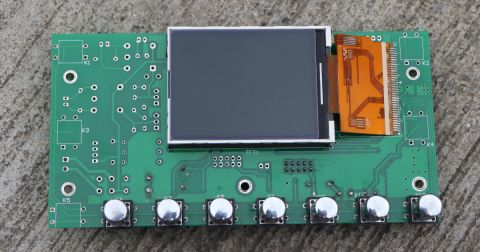
The image below shows an example of a flex PCB layer stackup that includes SMT components on one layer. You can see that there is no stiffener, so it is possible to place components in the flex region and solder them successfully. In this case, there is a lot of copper pour (probably for power) which helps to stiffen this that region of the board.

Solder lands - Solder lands need to be placed in the signal layer directly below the coverlay, and the coverlay needs to have holes punched so that SMT components can access the signal layer. Always check with your fabricator and make sure that their capabilities will accommodate your design choice. Always avoid placing these features and components directly in the bend area, and place components so that the length of the component is parallel with the bend.
Button Plating - An alternative method for defining lands for SMD components on a flexible region involves button plating. The signal layer still needs to be placed below the coverlay in the stackup, and punched holes in the coverlay are also used to access the signal layer. A through hole via is placed in the mounting pad, and the structure is then plated up to a specific thickness; this forms a strong solid copper foundation for mounting SMD components on the flex ribbon as the solid copper will have better ability to resist deformation during flexing. If the holes are left open, through hole components could also be placed on the flex ribbon.
Strain Relief
Another feature in the rigid-flex layer stackup that is not often discussed is the application of strain relief. A strain relief region helps to prevent mechanical stress from concentrating on the materials in the flex region at the rigid-to-flex transition. Without proper strain relief, any excessive bending or vibration can crack copper entering the rigid section. It’s also possible to delaminate the coverlay, barrel and pad failures can occur at the interface.
Strain relief is achieved by managing the stiffness at the transitions:
- Tapering copper pours and hatched planes as they enter the flex region
- Using multiple rigid terminations spread around the flex ribbon for mounting/fixation
- Apply a bead of epoxy along the flex/rigid transition to force a larger bending radius
- Remove unnecessary copper and vias near the transition region
As long as you can ensure bending occurs in the intended flex zone rather than at the interface, you can prevent the flex ribbon from tearing at a flex/rigid transition.

Rigid-flex design with a central rigid region, which can provide strain relief across the flex/rigid transition zones. Image source: Panda PCB.
Another area where strain can concentrate is in a bifurcation of the flex ribbon, where a ribbon branches off into different directions but without the use of a rigid region. The placement of a bifurcation in the middle of a flex ribbon should include a curved region to sufficiently separate the two flex sections.
Why would we not split the ribbon directly? This is because a cut into the ribbon without strain relief creates a region that can easily tear along a sharp edge. By placing a small curved region, the flex ribbon is much less likely to tear as the curved edge will prevent shearing along the ribbon edges.
Vias in Flex Designs
One important piece of information that is deeply related to the flex/rigid-flex stackup is the use of vias. The via geometry depends primarily on the overall thickness of the stackup and what qualification or standard you are designing towards (e.g., IPC Class 2 or 3).
Technically, any of the typical via geometries can be used in flex designs:
- Standard through-holes
- Blind/buried vias with sub-laminations
- Blind/buried vias for HDI
Via fabrication will be required to follow the standard aspect ratio rules for mechanical drilling and laser drilling. In terms of location of vias, if you want to use through-hole vias in a rigid-flex design, you should do it in the rigid region. If any vias are used in the flex region, that region should be fixated so that there is no chance that bending of the flex ribbon will fracture the vias. This is a topic I’ll discuss in another article.
Whether you need to build reliable power electronics or advanced digital systems, use Altium’s complete set of PCB design features and world-class CAD tools. Altium provides the world’s premier electronic product development platform, complete with the industry’s best PCB design tools and cross-disciplinary collaboration features for advanced design teams. Contact an expert at Altium today!

About Author
Related Resources
Related Technical Documentation
Table of Contents
Design to Release, Without the Friction
- Keep reviews tied to the right version
- Reduce handoff confusion and rework
- Spot sourcing and release risk earlier
- Work solo, share when needed
Get Started
Thank you, you are now subscribed to updates.

