PCB Noise Reduction: Do You Need Isolation, Shielding, or Filters?

Of all the noise and operational challenges designers face in their PCBs, there is one overarching problem that is arguably most popular: electronic noise. Any noise you pinpoint in your system could have one or many possible causes and solutions. It could originate as an SI/PI problem, it could possibly arise from some external source, or it could be good old-fashioned crosstalk!
Whenever some noise is measured on signals and it presents some operating problem for the system as a whole, what solutions should you use? These tend to fall into three categories: adding shielding, doing something to create isolation, or placing filters. Let's look at all of these as they tend to be the default solution set when confronted with many noise problems.
Step 1: Identify the Source
It might sound obvious, but before you start experimenting with any kind of filtering or shielding to reduce noise, you should make an attempt to identify the source of the noise in your system. You'd be surprised how often I get a question about noise, and yet there has been no investigation into what might be causing the problem to begin with. Don't skip the investigation and go straight to a solution, take time to identify the source.
As it turns out, if your noise is originating from something like a power integrity problem in a digital system for example, any of the three default options (filtering, isolation, and shielding) will do nothing to solve the problem. This is a stackup and layout problem, plain and simple. However, if you're dealing with something like a power system that is allowing too much noise to pass between power stages, a simple filter circuit might be all you need. Take some steps to narrow down the type of noise with some simple measurements, or at minimum to diagnose the location of the problem:
- Take direct measurements; even low-cost oscilloscopes or a simple multimeter might pinpoint the problem (e.g., ground bounce, excessive AC ripple, etc.)
- Start at the problem and work backwards to the signal source; noise problems usually start upstream from the point where the problem is noticed

Filtering
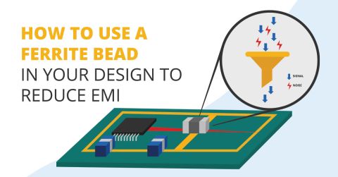
Filtering circuits and components are best used when you only want a specific frequency or range of frequencies to reach the load end of an interconnect. Flip this around; filters can also be used to remove one specific problem frequency from an interconnect (e.g., a notch filter). Filtering is best left to the analog or RF designer; you should not use filter circuits to try and remvoe noise from an interconnect carrying digital signals. For RF and analog systems, bandpass filtering is typically used to pass signals into a receiver and prevent noise.
Power systems will also make use of filters, primarily on the output stage of a regulator or the input stage where the device is connected to the main (unregulated) power source. In this usage, the filter is applied to try and remove conducted common-mode currents. Note that switching regulator topologies have a built-in filter from the inductance. If you have too much noise on the output from your regulator stage, you might need to increase the regulator's inductance (assuming you've already laid out the board correctly).
Isolation
This term is a bit ambiguous and is probably overused when we talk about noise. It often comes up in the context of mixed-signal PCB layouts. From what I can tell, this refers to two possible courses of action:
- Splitting the system so that it sits on top of two different ground planes
- Separating nets from each other so that there is less crosstalk
For mixed-signal systems, if you follow some basic layout principles surrounding placement and routing, you won't need to do something undesirable like splitting a ground plane. Separating nets is always a good way to prevent crosstalk or interference that might appear as noise on the system IOs.
Shielding
This should be a last resort to try and remove noise. There are many components in a PCB layout that can create a noise problem, and so it is tempting to just target those components with shielding and ignore everything else. Before using shielding, check the list of recommendations below first, then consider playing with some shielding options.

In the case you do find that you need shielding to overcome your noise problem and pass EMC testing, there are some commercially available shielding options:
- Custom shielding cans that will cover components and connect to ground
- Shielding gaskets, compounds, and meshes
- Ferrite plates that can be placed in an enclosure
The simplest form of shielding probably already exists in your PCB: your ground plane. Simply reworking the stackup to put the ground plane closer to your components, or adding a ground plane when there was none, will provide additional shielding.
Simple Digital Example
As is often the case, the best PCB noise reduction solution might involve multiple steps. Consider the snapshot of the dense layout for a digital board shown below. Suppose the problem is crosstalk between two nets, causing a glitch to appear on one of the IOs. There are two good solutions to the problem:
- Create more shielding by moving the reference plane closer to the layer with the victim net. This will reduce the mutual parasitics that create coupling between the aggressor and victim nets.
- Increase the spacing betwen the aggressor and victim nets. This will also reduce mutual parasitics between the nets.
#1 will be easiest to implement by far. Filters might be effective for removing some of the power carried by the noise glitch, but if this is a digital system, then the filter will also remove some of the signal, and it might not be read properly at the receiving component's IO.
In some dense layouts, the best PCB noise reduction method is to move the reference plane closer to your surface layer and to separate components from each other.
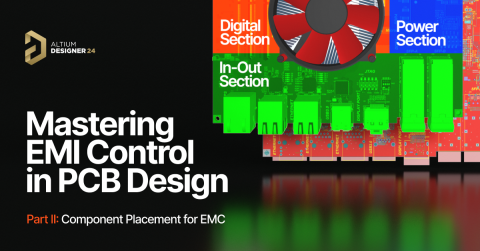
It Starts With Stackup and Placement
While it is true that specific noise problems can be solved with a bit of targeted shielding or filtering, the typical crosstalk and EMI problems you'll find in most boards won't be solved by placing filters. EMI problems like crosstalk, excessive radiated emissions, power glitches, signal glitches, and even some conducted emissions can be solved with smart layout and placement. If you get the stackup and placement correct, you won't have to worry about filters, silly things like guard traces, or shielding materials. Instead, focus on a few simple rules:
- Place your PCB ground plane or polygons near signals
- Plan a grounding strategy that considers your specific signal frequencies
- Route signals while maintaining references with well-defined return paths along each route
- Learn to spot parasitics that will affect your signals, specifically high dV/dt and dI/dt nodes and loops
- Learn about the factors that could create noise in your specific circuits or system
When you’re ready to implement solutions to your noise problems with powerful tool sets, use the PCB design features in Altium Designer®. Whether you need to place filters or modify your board to create isolation, your team will have access to everything needed to build advanced electronics in a single program. When you're ready to release your designs to your collaborators or to a manufacturer, you can use the secure collaboration features in the Altium 365™ platform. Everything you need to design and produce advanced electronics can be found in one software package.
We have only scratched the surface of what is possible to do with Altium Designer on Altium 365. Start your free trial of Altium Designer + Altium 365 today.

