


PCB Design Process: The EDA Design Approach

At a Glance
Streamline your PCB design process with EDA. Align requirements, schematic, layout, and release to cut respins and boost first-pass yield.


Hardware teams succeed when they can move from requirements to a working, manufacturable board with as few respins as possible. Electronic design automation (EDA) delivers on that goal by providing an integrated, constraint-driven workflow that keeps electrical, mechanical, and manufacturing requirements aligned from the first block diagram to the final release.
EDA replaces manual drafting and isolated simulators with a unified environment for requirements capture, schematic entry, simulation, PCB layout and routing, verification, and manufacturing documentation. When EDA software is well chosen and properly configured, it shortens design cycles and improves first-pass yield.
Key Takeaways
- EDA unifies the PCB workflow. A single, constraint-driven data model connecting requirements, schematic, simulation, layout, verification, and release helps reduce respins and improve first-pass yield.
- Standardization should be measurable. Build shared libraries and constraint sets, integrate with MCAD and PLM, then track spins per project, first-pass yield, and time from schematic freeze to release.
- Integration is now a baseline expectation. A modern EDA environment should connect cleanly with MCAD, PDM, PLM, and analysis tools so electrical, mechanical, and manufacturing teams can work from current data to reduce late-stage surprises.
- Unified context is a differentiator. The Altium platform connects Octopart Discover for solution exploration, Altium Develop for PCB design, and Altium Agile for enterprise workflows into a coordinated environment for distributed hardware teams.
What Is EDA Design in PCB Engineering?
EDA software is used to design, simulate, verify, and prepare electronic systems for manufacturing. In PCB engineering, EDA design typically covers:
- Requirements and system architecture
- Schematic capture and logical connectivity
- Simulation and analysis
- PCB layout and routing
- Verification and sign-off
- Documentation and release
Most EDA software is highly specialized to a specific area of design; only a few applications can address all aspects of product development. Traditional flows pushed each stage into a separate tool, with manual handoffs between them. Modern EDA design automation ties them together with a single data model, so connectivity, constraints, libraries, and manufacturing outputs all come from one project.
What Are the Popular EDA Tools for Electronic Design?
Electronic design automation companies offer tools that cluster into three broad groups.
- Entry-level and cost-constrained tools
- CircuitMaker gives users a free platform for designing with a toolset that is very similar to Altium Designer and includes a free personal workspace in Altium 365.
- KiCad provides a capable open-source suite for schematic, PCB, and basic 3D. It’s used in education, hobby work, and early-stage startups.
- EasyEDA and similar browser-based tools offer cloud-hosted schematic and PCB design, often tied to low-cost manufacturing.
- Professional environments
- Altium Develop is a flagship solution on the Altium platform for professional PCB teams. It support very large designs, advanced constraints, and deep integration with supply chain required in automotive, aerospace, and medical products.
- Cadence OrCAD, Siemens PADS, and Zuken CR-8000 also target professional design with capture and layout, plus optional analysis modules.
- Enterprise platforms
- Altium Agile includes the core feature set in Altium Develop and extends it into the enterprise data management domain. The advanced management features are available in the cloud or as an on-premises deployment.
- Cadence Allegro and Siemens Xpedition are heavier platforms which support large designs.
Beginners and hobby users often start with KiCad, EasyEDA, or CircuitMaker as these are free entry-level. Production teams tend to standardize on Altium, OrCAD, PADS, or higher-end enterprise platforms as board complexity and compliance demands increase.
Can EDA Design Automation Be Integrated with Other Tools?
Successful hardware projects demand coordination between electrical, mechanical, and procurement/manufacturing at every stage. Effective EDA design assumes tight integration with product data management (PDM), product lifecycle management (PLM), mechanical CAD (MCAD), and analysis tools.
ECAD and MCAD integration
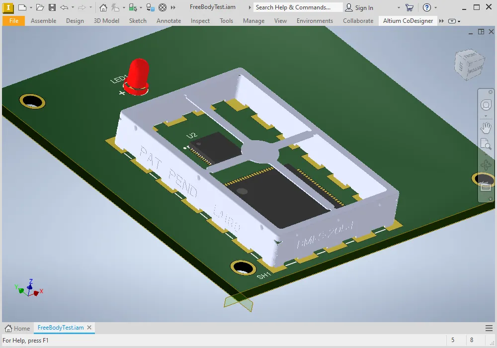
Three-dimensional formats and ECAD–MCAD collaboration make it easier to share board outlines, keepouts, component bodies, rigid-flex regions, and multiboard assemblies. In Altium Develop, ECAD–MCAD collaboration is built into the core environment with the MCAD CoDesigner, so PCB and mechanical teams can exchange changes without manual file shuffling, and both sides see the same revision history.
PLM and PDM integration
PLM and PDM systems serve as the official record for parts, bill of materials (BOM), and revisions. When EDA design software integrates with PLM, it can push structured BOM data into the system of record, tie releases to specific design revisions, and align engineering change requests with the live project. On the Altium platform, Altium Agile provides workflow automation, governance, and deeper connectivity to enterprise systems such as PLM and Jira.
Simulation, manufacturing, and test
Leading EDA environments also integrate with signal- and power-integrity solvers, netlist-based test systems, and external design-for-manufacturability (DFM) tools.
What Are the Main Features of EDA Design Automation Tools?
Most EDA design software for PCB engineering shares a common foundation. Key features to look for are:
- Unified design database
Schematic, PCB layout, 3D models, and manufacturing outputs share one underlying project representation. This is central to Altium Develop on the Altium platform, where all views and outputs come from the same data. - Constraint management and rule engines
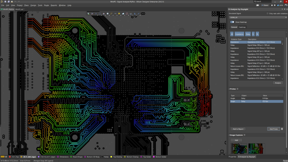
Rules cover net classes, physical clearances, impedance and length targets, via usage, differential pairs, and manufacturability limits. Constraint systems apply these in schematic and layout, and rule checks automatically verify compliance. - Integrated simulation and analysis
Schematic-level simulation and layout-aware signal-integrity (SI) and power-integrity (PI) analysis help identify functional and power-distribution issues before fabrication. - Interactive and assisted routing
Routing engines enforce constraints while supporting efficient workflows. Capabilities often include guided differential-pair routing, length tuning, and advanced via strategies, sometimes with automated assistance. - Three-dimensional visualization and ECAD-MCAD features
Three-dimensional board views help validate heights, clearances, and rigid-flex behavior. In Altium Develop, 3D views are tightly integrated with the PCB editor, so designers can switch between detailed 2D editing and full 3D assemblies. - DFx and manufacturing documentation
DFx tools analyze manufacturability and testability while the EDA tool generates fabrication and assembly outputs, including Gerber or ODB++ files, drill data, stackup and assembly drawings, and placement files. Such documentation is built into Altium Develop, rather than requiring an external add-on. - Library, data management, and collaboration
Central libraries, cloud workspaces, revision control, reviews, and APIs help teams manage parts and projects at scale. The Altium platform, delivered through Altium Develop and Altium Agile, is a prominent example of this approach.
How Does EDA Automation Improve Electronic Design Processes?
EDA design automation changes the PCB lifecycle by moving checks earlier, keeping intent aligned with implementation, and reducing data drift.
Moves critical checks earlier
Electrical rule checks, early simulation, and constraint setup push quality work into the front of the project. Designers validate the architecture and component choices before committing to layout, reducing downstream iterations.
Keeps intent and implementation aligned
Constraint systems ensure that the rules agreed upon during requirements and architecture drive placement and routing. In Altium Develop, the same rule set applies across schematic, PCB, and manufacturing outputs, so electrical intent and physical implementation remain consistent.
Reduces manual translation and data drift
Tight integration with MCAD, PLM, and manufacturing reduces manual data exports and re-entry. BOMs and documentation are sourced from the authoritative design database, and cloud-based sharing tools keep everyone on the same revision.
How to Choose and Standardize an EDA Environment
To consistently achieve these benefits, you need an EDA design environment that supports a unified flow. When you evaluate options, consider:
- Board complexity, performance targets, and regulatory requirements
- Team size, geographic distribution, and collaboration needs
- Integration requirements with MCAD, PLM, and external analysis tools
- Whether you prefer a single unified application or a loose stack of modules
The Altium platform, delivered through Octopart Discover, Altium Develop, and Altium Agile, combines a single design interface, strong 3D and ECAD-MCAD capabilities, integrated manufacturing outputs, and a cloud platform for collaboration and lifecycle management. Other popular EDA tools for electronic design might be able to meet similar needs, especially in very large enterprises with large budgets, but often with a heavier dependence on separate databases and toolchains.
For most PCB organizations, a practical path is to choose an EDA design platform that covers requirements, schematic, simulation, layout, verification, and release in one environment; build shared libraries and constraints; integrate with mechanical and data systems; and track metrics such as spins per project, first-pass yield, and time from schematic freeze to release. If those numbers improve quarter by quarter, your EDA automation strategy is working.
Frequently Asked Questions
1. What is EDA design in PCB engineering?
EDA design in PCB engineering is the use of electronic design automation software to manage the full lifecycle of a board, including requirements capture, schematic capture, simulation, PCB layout and routing, verification, and manufacturing release. The goal is to keep all these stages within a single constraint-driven environment rather than using separate tools.
2. How does EDA design software fit into the overall PCB design process?
EDA design software is the backbone of the PCB workflow. It translates product and electrical requirements into schematics, validates behavior with simulation, implements the physical board, checks it against electrical and manufacturing rules, and generates fabrication and assembly outputs from a shared project and library set.
3. How is Altium different from other popular EDA tools for electronic design?
Altium delivers its capabilities through the Altium platform with three connected solutions: Octopart Discover for solution and component exploration, Altium Develop as the primary PCB and system design environment, and Altium Agile for enterprise workflows and integrations. Together, they provide one context for schematic, PCB layout, 3D, constraints, supply-chain intelligence, and documentation, reducing the need to stitch together multiple tools.
4. When should a team move from entry-level tools to a professional EDA environment?
Teams typically need a professional EDA environment once boards become faster, denser, or more regulated, and respins start to pile up. At that point, professional EDA design software such as Altium Develop, offers stronger constraints, better 3D integration, more robust documentation, and tighter collaboration.
5. What are the benefits of EDA design software integrated with MCAD and PLM systems?
EDA design software integrates with MCAD so mechanical and electrical teams can share the same geometry and component models. With PLM integration, BOMs, part data, and revisions flow into the enterprise system of record. On the Altium platform, Altium Develop handles day-to-day ECAD-MCAD collaboration, and Altium Agile focuses on data management, PLM connectivity, and hardware workflows.
6. What features should I prioritize when evaluating EDA software for high-speed or complex boards?
Prioritize constraint management and analysis. You need strong support for net classes, impedance control, length matching, differential pairs, via rules, and manufacturability rules, plus accessible signal- and power-integrity analysis tied to the actual layout. A unified environment, such as Altium Develop, makes it easier to apply and verify those constraints consistently.
7. How does cloud-based collaboration change the way PCB teams use EDA tools?
Cloud-based collaboration turns PCB design into a shared workspace where projects, libraries, and outputs stay up to date and accessible to the right people. On the Altium platform, Altium Develop and Altium Agile provide browser-based views, controlled sharing, and integrated comments to reduce file emailing and keep distributed teams aligned.
8. How should a team plan migration to a standardized EDA design environment such as Altium?
A practical approach includes picking pilot projects, setting success metrics, building shared libraries and constraint templates in the new environment, then training the team and running those pilots while refining workflows. Standardizing on the Altium platform lets you set up this infrastructure once and reuse it across products. Existing Altium customers can migrate to Discover, Develop, and Agile on the same platform that already hosts their designs.

About Author
Related Resources
Table of Contents
- Key Takeaways
- What Is EDA Design in PCB Engineering?
- What Are the Popular EDA Tools for Electronic Design?
- Can EDA Design Automation Be Integrated with Other Tools?
- ECAD and MCAD integration
- PLM and PDM integration
- Simulation, manufacturing, and test
- What Are the Main Features of EDA Design Automation Tools?
- How Does EDA Automation Improve Electronic Design Processes?
- Moves critical checks earlier
- Keeps intent and implementation aligned
- Reduces manual translation and data drift
- How to Choose and Standardize an EDA Environment
- Frequently Asked Questions
- 1. What is EDA design in PCB engineering?
- 2. How does EDA design software fit into the overall PCB design process?
- 3. How is Altium different from other popular EDA tools for electronic design?
- 4. When should a team move from entry-level tools to a professional EDA environment?
- 5. What are the benefits of EDA design software integrated with MCAD and PLM systems?
- 6. What features should I prioritize when evaluating EDA software for high-speed or complex boards?
- 7. How does cloud-based collaboration change the way PCB teams use EDA tools?
- 8. How should a team plan migration to a standardized EDA design environment such as Altium?
Design to Release, Without the Friction
- Keep reviews tied to the right version
- Reduce handoff confusion and rework
- Spot sourcing and release risk earlier
- Work solo, share when needed
Get Started
Thank you, you are now subscribed to updates.

