


The Best Electronic Design Automation (EDA) Software for PCB Design


You don’t have time for underperforming electronic design automation (EDA) tools that are difficult to learn and use, you need the best EDA software for PCB design automation that you can get; Altium Designer, available within Altium Develop. But what is EDA software?
You’ve got a job that needs to be done and that means the printed circuit board design is your responsibility. You don’t have time for EDA PCB design tools that are underpowered and second-rate, nor do you have time to learn how to use difficult and complex electronic design automation tools. You need quality PCB design software that is self-contained with all of the EDA tools for PCB design needed for the job and is naturally intuitive so that your learning curve will be minimal. The PCB design tool that you are looking for is Altium Designer.
From schematic to layout with simulators and productivity enhancement features, Altium Designer is a full set of PCB design tools that were created for engineers like you. Its intuitive and easy-to-use features are built on a powerful platform designed to seamlessly integrate all its design automation tools into a single comprehensive design flow. Whether you are retrieving the latest component data from your vendors, running your integrated circuits through the simulators, capturing the schematic, laying out the board, or creating automated batch manufacturing files, Altium Designer is the best EDA software for PCB design automation.
What is Electronic Design Automation (EDA)?
Electronic Design Automation (EDA) refers to a category of software tools used by engineers to design, simulate, verify, and manufacture electronic systems. Ranging from integrated circuits (ICs) to printed circuit boards (PCBs), EDA software automates the complex steps of hardware development, ensuring that designs perform correctly before they are physically built.
The Main Categories of EDA Tools
While many engineers use "EDA" and "ECAD" interchangeably, Electronic Design Automation actually encompasses a much wider ecosystem of software. A complete EDA software workflow typically relies on three distinct pillars to bring a product from concept to reality:
1. Simulation & Verification Tools
Before a single component is placed, EDA tools are used to model circuit behavior. This includes SPICE simulation for analog circuits, signal integrity analysis for high-speed digital lines, and power integrity checks. The goal is to verify the logic and physics of the design virtually, preventing costly hardware prototypes.
2. Physical Design (ECAD/Layout)
This is the most visible part of the electronic design automation software stack. It involves the physical placement of components and the routing of copper traces on the Printed Circuit Board (PCB) or Integrated Circuit (IC). Advanced EDA electronic design automation platforms like Altium Designer integrate this stage directly with the schematic, ensuring that physical constraints (like board shape and layer stackup) are respected.
3. Manufacturing & Output Generation
The final stage of the EDA process automates the creation of production data. This includes generating Gerber files, Bill of Materials (BOM), and pick-and-place files. Modern EDA tools now integrate directly with supply chain databases to validate part availability in real-time during this phase, rather than after the design is finished.
It All Starts with a Solid EDA Software Foundation
Structures built on shifting sands usually don’t last, and that is why we at Altium have created the most solid EDA software platform foundation possible for Altium Designer. Built on the powerful architecture of the 64-bit multi-threading system, Altium Designer has what you need to complete any Printed Circuit Board design project.
Anchored on that powerful platform is Altium EDA Designer’s signature unified design environment, which establishes a commonality of the data between the tools. This allows you to work without fear of corrupted data and provides common user interface components between the design automation tools, helping you to work more efficiently. The unified design environment also gives you the added benefit of superior global editing, where the changes you make in one tool will be propagated throughout your design database to all of the other computer-aided design tools in Altium EDA Designer.
Circuit Simulation Built from the Ground Up for Success
Altium Designer has been created by engineers for engineers so it has the features and functionality within it that you need for your work.
- Altium Designer’s unified design environment has been specially developed to create a common working design environment to make your job easier and more efficient.
Learn More about Altium Designer’s unified design environment.
- With Altium Designer’s unified design environment, the changes you make in one tool are propagated throughout the system to every other tool.
- Here’s more on how a quality set of EDA tools for PCB design based on a unified design environment can make you more productive and successful.

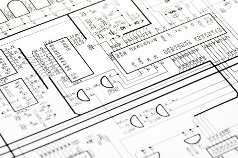
Altium Designer’s schematic capture tools are easy to learn and use, yet yield powerful results
Powerful and Versatile Schematic Capture Software
Altium Designer’s schematic capture has been created to help users come up to speed quickly. In a very short amount of time, you will find yourself mastering the art of schematic creation in Altium Designer. From there the sky’s the limit because Altium Designer has also been created to handle the most complicated designs. Not only will you be able to create large complex multi-channel hierarchical designs, but you will also be able to specify all of your design rules from within the schematic.
This will give you the control you need over the layout so that the finished circuit board will be built the way you designed it. You also will have greater control over the parts you use with Active BOM. This tool not only gives you an additional portal into your design data by managing your components in an easy-to-use interface, but it will also give you cloud connections to your vendors. You will be able to verify current pricing, availability, and the latest data sheets for the parts that you are using in your schematic.
From Your EDA Software PCB Ideas to the Design Database, Your Schematic Capture Tools Need to Work for You
Altium Designer’s schematic capture tools allow you to design your circuits the way you want them to be instead of constraining you with restrictions.
- Altium Designer’s schematic capture application is easy to learn and use while at the same time powerful enough for your most challenging electronic designs.
- Check online for the status of your parts, manage your design components across the tools, and create a superior bill of materials report. BOM Management is the capability you need.
Learn More about real-time BOM management in Altium Develop.

Layout in Altium Designer is complemented by the powerful 3D environment
The Best EDA Tools You Can Get for PCB Layout
When it comes time for layout, Altium Designer’s layout editor will handle any level of design technology that your schematic will drive. Altium Designer’s part placement functionality will allow you to easily and efficiently place and align your parts to whatever grid and spacing that you need.
Altium Designer’s vast interactive, auto-interactive, and auto-routing tools will then quickly get you to 100% route completion. When your layout is completed, Altium Designer also features many different output tools from batch job output files to automated manufacturing drawing generators. In every way, Altium Designer has been created to help you design the best possible Printed Circuit Board possible.
Frequently Asked Questions about EDA Software
Q: What is the main purpose of EDA software?
The primary purpose of EDA (Electronic Design Automation) software is to streamline the design, simulation, and manufacturing of electronic systems. It replaces manual drafting with automated processes that ensure accuracy in complex integrated circuits (ICs) and printed circuit boards (PCBs).
Q: What is the difference between ECAD and EDA?
While often used interchangeably, EDA is the broader industry term encompassing chip design, FPGA, and board-level design. ECAD (Electronic Computer-Aided Design) typically refers specifically to the physical layout and mechanical aspects of the PCB design process.
Q: Are EDA tools only used for chip design?
No. While EDA originated in the semiconductor industry for designing transistors on silicon, modern electronic design automation software is the standard for designing printed circuit boards (PCBs), multi-board systems, and electronic product enclosures.
Q: Can EDA software simulate real-world conditions?
Yes. Advanced EDA tools include simulation engines for Signal Integrity (SI), Power Integrity (PI), and 3D electromagnetic analysis to predict how a device will perform under real-world electrical and physical stress.
Design Your PCB Layout Right Every Time
Altium Designer has everything built into it for quality electronic design automation PCB layout, from parts placement to routing to manufacturing output files.
- Altium Designer has been configured with placement features and functionality to help you align your parts the way you want them to be.
Learn More about smart component placement in Altium Designer.
- Trace routing has never been easier with the different routing capabilities within Altium Designer.
Learn More about Altium Designer’s intelligent routing capabilities.
- Altium Designer handles the heavy lifting of creating manufacturing output files, freeing you more time to design the electronic board.
Learn More about auto-generating manufacturing drawings with Draftsman.
There’s no need to get frustrated with PCB design tools that are incomplete or not up to the challenge. You also don’t need to spend your valuable time and money on EDA tools that are difficult to learn and use. Instead, take a good look at the best EDA software for Printed Circuit Board design; Altium Designer.
Whether you need to build reliable power electronics or advanced digital systems, Altium Develop unites every discipline into one collaborative force. Free from silos. Free from limits. It’s where engineers, designers, and innovators work as one to co-create without constraints. Experience Altium Develop today!

About Author
Related Resources
Related Technical Documentation
Table of Contents
- It All Starts with a Solid EDA Software Foundation
- Circuit Simulation Built from the Ground Up for Success
- Powerful and Versatile Schematic Capture Software
- From Your EDA Software PCB Ideas to the Design Database, Your Schematic Capture Tools Need to Work for You
- The Best EDA Tools You Can Get for PCB Layout
- Design it Right Every Time
Design to Release, Without the Friction
- Keep reviews tied to the right version
- Reduce handoff confusion and rework
- Spot sourcing and release risk earlier
- Work solo, share when needed
Get Started
Thank you, you are now subscribed to updates.


