


PCB Developing: Preparing Your Circuit Board for a PCB Etching Service


There are times where you don’t need to produce a finalized, silk-screened board at high volume, and you may only need to use a blank PCB with no components or silkscreen. Blank PCBs can be useful for prototyping, breadboarding, experimenting with components, and accessing external traces. These boards do not need to go through a special production process, they only need a limited documentation package to begin fabrication.
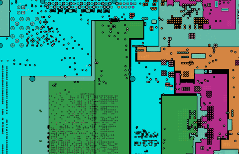
ALTIUM DESIGNER®
The industry’s only design application that offers a complete set of design tools for circuit board layout and manufacturing preparation.
Your next circuit board might only need to be produced at low volume and without assembled components. If you are simply looking for a board to use for proof-of-concept testing, basic prototyping, or breadboarding, a bare circuit board without components is a simple solution. A PCB etching service can prepare these bare boards for you with a reduced fabrication process and no assembly.
To get your new design prepared for fabrication with a PCB etching service, you’ll need to prepare several pieces of documentation. Your design will also need to be prepared in the same way as any other board, complete with planes, traces, pads, and PCB footprints clearly placed in a PCB layout. With the production planning features in Altium Designer, you can prepare your PCB layout and Gerber files your PCB etching service will need to produce your board.
Documentation Needed for a PCB Etching Service
Complete PCBAs will need a thorough set of documentation that includes fabrication and assembly instructions, test requirements, sourcing data, and project files. Your design documentation package needs to include the following information:
- CAD files
- Gerber files (RS-274-D and RS-274X)
- Bill of materials with sourcing data
- Fabrication and stackup drawings
- Drill drawings and CNC drilling instructions
- Pick-and-place files for automated assembly
- Netlists and testpoint information
A PCB etching service only needs a reduced set of documentation to properly produce your board. Specifically, your etching service will need your CAD files, Gerber files, drill and fab drawings, and any test requirements. If you can easily produce these files from your PCB layout data, you can quickly prepare an order for bare circuit boards through a PCB etching service.
Quickly Generate Fabrication Files in Altium Designer
When you use Altium Designer, you’ll have a design application that integrates manufacturing preparation with circuit board design and layout. Altium Designer will generate Gerber files and other fabrication data directly from your PCB layout data without the need for an additional design application. Altium Designer makes it easy to create a complete documentation package for any PCB manufacturer in a matter of minutes.
- Gerber files are central to the PCB fabrication process as they are used to create bare circuit boards before assembly.
- Some fabricators and PCB etching service companies will support alternative vendor-neutral file formats for PCB fabrication and etching.
- Altium Designer includes the fabrication file tools you need alongside your circuit board design tools and documentation features.
Learn more about generating PCB fabrication files in Altium Designer.

Altium Designer’s fabrication and CAM features help you prepare high-quality Gerber files for a PCB etching service or full-scale fabrication.
The Design Tools You Need for PCB Etching
Even though a PCB etching service uses a reduced manufacturing process to create a bare circuit board, designers need the same tools they would use to create a complete PCBA. Some of the important design tools needed for circuit board design and etching preparation include:
- CAD tools for schematic sheet design and PCB layout
- Schematic capture tool for importing components into a blank circuit board
- Component search and selection features
- PCB footprint creation and library creation tools
Once your PCB layout is finished, you can easily create your manufacturing files when you use an integrated circuit board design application. Only Altium Designer creates the integrated environment design teams need to prepare boards for a PCB etching service.
Altium Designer Unifies PCB Layout and Manufacturing
Because Altium Designer integrates important tools for PCB design and manufacturing into a single program, it’s simple to generate manufacturing files directly from PCB layout data. The unified environment in Altium Designer integrates all the important design tools engineers need to prepare for manufacturing in a single program.
- Use the Manufacturer Part Search panel in Altium Designer to the PCB footprints you need for a bare circuit board.
Learn more about the Manufacturer Part Search panel in Altium Designer.
- Your circuit board layout needs to include PCB footprints that accurately reflect component specifications. This will ensure your PCB etching service can create your board correctly.
Learn more about finding and creating footprints in Altium Designer.
- Altium Designer helps you do more than just create PCB etching files, you can move through the entire circuit board design process in a single application.
Learn more about creating a circuit board layout in Altium Designer.

You can take control of your entire design process in Altium Designer’s integrated PCB environment.
Complete Design and Production Planning in Altium Designer
With the complete set of PCB layout and fabrication features in Altium Designer, a design team or an individual design will have everything needed to produce a simple board with a PCB etching service or a volume run at millions of units. From schematics to PCB layouts and manufacturing files, you’ll have everything needed to create cutting-edge electronics. Altium Designer also goes above other PCB design software applications by integrating with a comprehensive cloud collaboration platform.
Altium Designer and Altium 365 Make Design and Fabrication Easy
The Altium 365 platform is the industry’s first comprehensive sharing, version control, and collaboration platform for PCB designers. A PCB design team can collaborate on their circuit board design projects from within Altium Designer, share their design libraries, and prepare projects for a PCB etching service. With Altium 365, it’s never been easier to share schematics, components, simulation models, PCB layout files, and manufacturing packages.
- When you need a single application with all tools for design and manufacturing, use Altium Designer. You can create cutting-edge technology in Altium Designer’s unified PCB design platform.
Learn more about printed circuit board design in Altium Designer’s unified environment.
- Altium Designer’s user interface helps you stay productive as you create your circuit board designs and prepare them for production.
Learn more about the complete set of design tools in Altium Designer.
- When you’re ready to share your design with your PCB etching service, use the Altium 365 platform. You can store and share all your PCB projects and manufacturing files in a single cloud-based platform.

Send your Altium Designer circuit board and Gerbers to a PCB etching service using the Altium 365 platform.
Altium Designer users can move through the entire design process, going from schematics to a PCB layout and manufacturing documentation. Whether you plan to produce bare prototype circuit board designs with a PCB etching service or a complete PCBA at volume, use Altium Designer to create your new board. Make the switch today to get access to the industry’s best circuit board design tools.
Altium Designer on Altium 365 delivers unprecedented integration to the electronics industry until now relegated to the world of software development, allowing designers to work from home and reach unprecedented levels of efficiency.
We have only scratched the surface of what is possible to do with Altium Designer on Altium 365. You can check the product page for a more in-depth feature description or one of the On-Demand Webinars.

About Author
Related Resources
Related Technical Documentation
Table of Contents
Design to Release, Without the Friction
- Keep reviews tied to the right version
- Reduce handoff confusion and rework
- Spot sourcing and release risk earlier
- Work solo, share when needed
Get Started
Thank you, you are now subscribed to updates.


