


PCB Layout Replication


PCB Layout Replication in Altium Designer® 24 effortlessly speeds up your entire design process. Duplicate layouts for recurring circuit blocks and component groups to boost efficiency while cutting costs. Learn more about this brand-new feature in our quick guide.
Introduction
In the realm of electronics, PCB Layout Replication emerges as a key process, vital for preserving the intricate functionalities of original designs in their duplicates. This technique goes beyond mere imitation, demanding a deep understanding of the original layout’s operational intricacies to ensure the replica performs equivalently.
This document delves into the core functionalities of PCB Layout Replication, highlighting the detailed processes that facilitate the accurate recreation of a PCB’s functional aspects. These include critical components such as exact part placement, connectivity fidelity, and precise heat distribution mapping, ensuring the replicated board meets the performance and reliability standards of the original.
Readers will be guided through the nuanced technicalities involved in this replication process, from initial analysis to the final production of a fully functional duplicate. Emphasis is placed on the importance of preserving operational integrity and how this practice contributes significantly to ongoing advancements in the electronics industry.
Benefits of Altium Designer PCB Layout Replication
- Efficiency in Design Duplication: PCB Layout Replication tools allow for the swift duplication of design elements, reducing the time and effort required to recreate complex circuits from scratch.
- Consistency and Reliability: Replicating proven PCB layouts ensures consistency in performance and quality, especially important in large-scale manufacturing or in producing subsequent batches of a tested design.
- Cost Reduction: By replicating existing designs, companies can save on the costs associated with new design creation, including labor, resources, and time, ultimately leading to lower production costs.
- Error Minimization: Using a tried-and-tested PCB layout reduces the likelihood of errors that might occur during the design phase, contributing to higher reliability of the final product.
- Simplified Troubleshooting: Working with a familiar layout simplifies the process of identifying and resolving issues, making maintenance more efficient.
- Faster Time-to-Market: PCB Layout Replication speeds up the design process, enabling faster production cycles and helping products reach the market more quickly.
- Easy documentation and compliance: Replicating an existing, compliant PCB layout eases the burden of documentation, ensuring that all replicated designs remain consistent with industry standards and regulations.
- Enhanced Scalability: Companies can more easily scale their operations up or down, thanks to the ease with which layouts can be replicated or modified for different production volumes.
PCB Layout Replication Use Case
PCB Layout Replication stands as a cornerstone in optimizing the design process, ensuring consistency, and expediting production in the PCB industry. It provides a streamlined solution for duplicating functional blocks, ensuring uniformity, and accommodating design specifications efficiently.

1. Select the elements that are used as a reference to the other blocks.
Here is an example of how PCB Layout Replication can be implemented in a practical scenario:
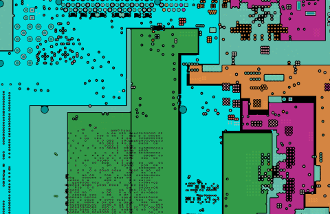
In a flat PCB design, the designer finalizes the first functional block. Instead of tediously copying and combining elements by hand for subsequent blocks, the designer uses the PCB Layout Replication tool. This tool will help quickly replicate the block, accurately transferring all details. The designer will quickly place these consistent replicas into a larger layout, saving time and ensuring consistent performance throughout the project.

2. Next, select PCB Layout Replication from the Tools menu.

3. In the PCB Layout Replication dialog, the components from the original block will appear in the Source Block section on the left, while the identified target block(s) will be displayed in the Target Blocks section on the right. You can reveal or conceal the list of components for each target block by expanding or collapsing its entry. To designate the target blocks for replication, utilize the checkboxes alongside each target block entry.

If the current selection fails to detect a target block, a warning dialog will appear to inform you. Ensure that the design and selection meet the necessary criteria for the components and their connectivity.

Note: If existing routing is found in a target block, it will appear under the Routing Detected category in the Target Blocks section of the dialog. These blocks are excluded from default replication, indicated by disabled checkboxes. However, if you decide to include such a block, be aware that existing intercomponent routing will be deleted. If the dialog’s Copy routed nets option is active, the source block’s routing will replace it, while unrouted objects in the target block will stay unchanged.
Conversely, Target blocks without detected routing will fall under the No Routing category and are set for replication by default, evidenced by enabled checkboxes.
4. In the Options section, check the appropriate checkbox to define which elements should be duplicated
- Copy routed nets - allows for the replication of copper objects like tracks, arcs, pads, vias, fills, regions, and polygons that link components in the original block.
- Copy Designator & Comment formatting - ensures that the formatting of designator and comment strings from the source block’s components is mirrored in the target blocks.
- Copy unrouted objects - enables the duplication of non-routing objects, including copper objects not connected to source block components, or those linked to just one component pad in the source block.
- Use interactive placement - dictates the method of target block placement post-replication:
- When disabled, each target block is automatically positioned in reference to the “main” component. By default, this is the component with the most pins, or the one with the largest area in the event of a tie. In the Source Block window, this main component is indicated by a symbol


Additionally, any component can be set as the main symbol by clicking on its respective row in the left column.
- If enabled, it allows for the manual positioning of each chosen target block.
5. The Preview area automatically refreshes to show changes in the target block when you toggle the options on or off.


6. After selecting the desired options, click Replicate. The arranged block is ready to be placed on the board
Conclusions
PCB Layout Replication revolutionizes the design process, enabling the instantaneous duplication of complex circuits, which accelerates the transition from concept to production. This efficiency reduces the overall time-to-market, giving your projects a crucial head start in today’s fast-paced environment.
The methodical replication of tried-and-true PCB layouts guarantees a standard of consistency and reliability previously unattainable. This approach not only minimizes the likelihood of errors during the design phase but also ensures the uniform performance of the end products, solidifying customer trust and satisfaction.
Through intelligent scalability and significant cost reductions, PCB Layout Replication transforms production economics. By eliminating the need for repeated, ground-up design work, resources are utilized where they matter most, optimizing production costs and enhancing the competitive edge of your business.
Safeguarding intellectual property is paramount in the digital age, and PCB Layout Replication is instrumental in this regard. By keeping the replication process in-house or within authorized entities, your valuable designs are protected from external threats, ensuring business continuity and sustained technological advantage.
Related Resources
Related Technical Documentation
Table of Contents
Design to Release, Without the Friction
- Keep reviews tied to the right version
- Reduce handoff confusion and rework
- Spot sourcing and release risk earlier
- Work solo, share when needed
Get Started
Thank you, you are now subscribed to updates.

