PCB Panelization Using The Embedded Board Array

Every designer is concerned with producing the highest quality product as efficiently and effectively as possible. When you’re preparing your design for your PCB manufacturer, you need to ensure your board complies with DFM and is ready for maximum yield. The standard practice is to use PCB panelization to manufacture an array of PCBs in parallel. The complete set of DFM features and panelization tools in Altium Designer will help you prepare for your next PCB manufacturing run and source components for your design. Here’s how you can get the most out of the PCB panelization features in Altium Designer.
ALTIUM DESIGNER
PCB design software enabling all of your design, manufacturing, and assembly processes.
You’ve completed your design, built and tested your prototype, and now your PCB design is ready for manufacturing. For this design, you need to specify how your manufacturer will fabricate your board. To do this you will need to create your own panel for the PCB design. Printed circuit board designs are put into standard panel sizes for manufacturing. These panels allow the board or boards to be smoothly run through the manufacturing process, and afterwards the boards are separated from each panel.
A panel has specific design requirements to ensure efficient printing and removal during PCB manufacturing, and you’ll need the right set of CAD tools for panel creation. Altium Designer has all the tools you need for the panelization of your PCB designs. You’ll have the tools needed to check your design for DFM violations and create a panel for an array of circuit boards. Take your new circuit board from design to manufacturing with Altium Designer.
Panelizing PCBs: Methods and Challenges
Creating a panel requires more than just drawing a rectangle around your board outline. You don’t need to simply copy and paste components between different regions in your PCB layout. In addition, multiple boards with the same stackup can share the same panel, and each board might be stepped and repeated on the same panel.
The goal in PCB panelization is to fit as many copies of a circuit board as possible into an array on a panel. The panel size is predetermined by your materials supplier or PCB manufacturer, so you need to work with your manufacturer to create your panels. Some manufacturers will do this for you, but you can save yourself some time and expense if you have the right design tools for PCB panelization.
The Tools You Need for PCB Panelization
Your PCB layout needs to be imported into your PCB panelization features and placed in a board array. You need to be able to rotate and flip boards so that you can fit the maximum number of boards into your panel. Once you’ve placed all your boards in your panel, you’ll need to generate a Gerber file for your panel so that it can be used to create a stencil for manufacturing.
- There are many steps required to prepare your design for full-scale manufacturing, and PCB panelization is just one of those steps.
- CAM tools in your PCB design software are critical for preparing an accurate circuit board array on a panel, which can then be exported as Gerber files.
Learn more about CAM features for PCB panelization in Altium Designer.
- With Altium Designer’s unified set of CAD tools, your PCB layout data is immediately brought into your PCB panelization tool for easy manufacturing preparation.
Learn some simple steps for PCB panelization in Altium Designer.
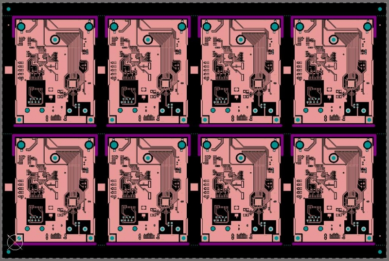
CAM data showing a circuit board array in a panel in Altium Designer.
Generating Your PCB Manufacturing Documentation
A PCB panel is an important piece of documentation, but you’ll need other documentation to get your PCB into production. Required documentation includes a list of parts and sourcing data in your bill of materials, which should also match the reference designators in your design files. PCB manufacturers could require design files, including panel drawings, in any number of formats. Your design software should be adaptable to accomodate any set of deliverables for PCB manufacturing.
File Formats for PCB Panelization and Documentation
Your design tools should give you everything you need to generate documentation in standard file formats. This includes files showing panel artwork, as well as universal design files and a bill of materials. You shouldn’t need an external set of design programs to generate this documentation; Altium Designer has everything you need for design, PCB panelization, documentation, and much more.
- Once you’ve created a panel for your circuit board, you need to produce other job output files, such as Gerber files, NC Drill, and ODB++.
- There are some important points to watch when creating PCB assembly documentation for a fabricator.
Learn more about PCB assembly documentation creation and PCB panelization.
- EMS companies expect a complete documentation package, including panelized circuit board arrays and Gerber files for your panel.
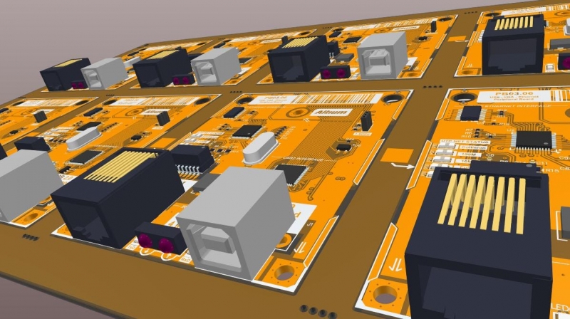
3D view of a PCB panel with the MCAD features in Altium Designer.
Get to PCB Manufacturing Quickly with Altium Designer
The goal of PCB design work is to create the best possible design for the least amount of money. This includes making the most cost effective component choices and designing your PCB to align with DFM guidelines. Altium Designer has all the functionality you need to create your PCB panel and reducing your overall PCB manufacturing costs. In addition, you’ll have access to a complete set of design and validation tools in Altium Designer’s integrated environment.
Design Your Circuit Board in Altium Designer’s Unified Environment
The rules-driven design engine in Altium Designer has all the design features you need to take your circuit board from idea to mass manufacturing and assembly. Everything you need to prepare a real circuit board, including PCB panelization, is included in Altium Designer. You won’t have to switch between different design applications to create your PCB assembly and fabrication drawings, everything you need is in one program.
- The CAD tools in Altium Designer’s rules-driven design engine are unified into a single program for complete design and manufacturing.
Learn more about the PCB design features in Altium Designer.
- Altium Designer includes an embedded board array tool for quickly creating a panel prior to manufacturing.
Learn more about PCB panelization with the embedded board array in Altium Designer.
- If you’ve never prepared a circuit board array on a panel, it helps to learn more about PCB panelization from an EMS expert.
Learn more about PCB panelization from EMS expert Kelly Dack.
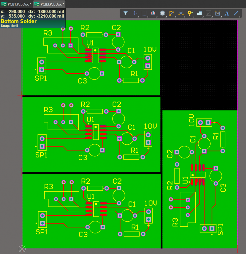
PCB panelization in Altium Designer
Increasing your yield and reducing cost is all about PCB panelization and proper DFM checks. Altium Designer gives you control over your DFM validation through its rules-driven design engine, and you’ll have the CAD tools you need to arrange a panel with copies of your circuit board. Finally, the deliverable generation tools give you everything needed to prepare for a full manufacturing run.
Altium Designer on Altium 365 delivers an unprecedented amount of integration to the electronics industry until now relegated to the world of software development, allowing designers to work from home and reach unprecedented levels of efficiency.
We have only scratched the surface of what is possible to do with Altium Designer on Altium 365. You can check the product page for a more in-depth feature description or one of the On-Demand Webinars.

