How to Estimate PCB and PCBA Pricing


If you look at different PCB manufacturer websites, you will see utilities where you can quote the cost to produce bare boards or assemblies. Try quoting the same board through two different manufacturers, and you shouldn't be surprised when you see two different prices. While we should expect prices to be similar across different manufacturers in the same region, there are differences in capability and service levels that lead to differences in PCB and PCBA pricing.
A factor in pricing that is often not considered is the BOM cost and the logistics cost. Ten years ago, shipping was almost an afterthought or it was small enough that it was lumped into the total cost of a production run. That is certainly not the case anymore due to changes in the structure of component supply chains and major changes in trade agreements between producer and consumer countries.
With this being the case, this article will be a deep dive on what drives PCB and PCBA pricing. The factors discussed here apply both domestically and internationally. While you can't directly control all the costs in a manufacturing run, some supply chain tools can help you assess the trade-offs in local or overseas production, helping you make the best PCB and PCBA pricing decisions.
What Drives Electronics Manufacturing Cost?
This is an important question that many designers don't often consider when choosing where to produce their designs. At a high level, the total cost (or landed cost) of a product depends on the following four factors:
- Capability, or the level of productivity in terms of machine time and labor required to produce a bare board or PCBA.
- Supply chain, or the availability of required components at competitive parts cost and low logistics cost.
- Service level, which refers to the number of add-on services requested as part of the production run.
- Subsidization, or the level to which governments provide support for their manufacturing base, allowing them to be much more cost-competitive in a global market.
For example, production overseas in China is known to be very inexpensive due to a combination of the above factors. Therefore, companies in the United States and Europe have to compete on other factors, such as local supply chain, logistics management, and/or service level. Domestic manufacturing with Western EMS companies has also benefited from export control restrictions for certain industries (e.g., ITAR for defense and aerospace), which creates a legal mandate to produce certain products domestically, either in part or in whole.
In addition to these four high-level factors, the relative proportion of total cost gets divided among the bare PCB, PCB assembly, and components. A typical breakdown is given below.
|
Manufacturing area |
Percentage of total cost |
|
PCB fabrication |
Up to 40% |
|
PCBA production |
Up to 50% |
|
PCB components |
Up to 80% |
These are huge ranges in terms of the relative costs of bare boards, assemblies, and the components in the BOM. But for most products, you can extract the trend shown in the table, where PCB fabrication cost is the lowest portion and either the assembly or the components is the largest portion. In particular, for designs with a large number of integrated circuits or specialized components, such as advanced ASICs or FPGAs, component costs can easily form the lion's share of the total product cost.
Manufacturing Capability as a PCB Pricing Driver
The copper features, clearances, and components placed in a PCB are also cost drivers in PCB manufacturing. These factors drive the cost of PCB and PCBA pricing due to the required capability to produce the design. The table below summarizes these cost drivers.
|
Copper feature size/clearance |
Higher cost due to usage of:
|
|
Drilling capability |
|
|
Sub-laminations |
More sub-laminations increases drill/press steps and total cost |
|
Sequential lamination |
More build-up layers increases cost |
|
Materials |
Low-Tg FR4 is least expensive. Higher cost due to usage of:
|
|
Backdrilling |
Higher precision controlled depth drilling increases cost |
|
Surface finishes |
|
|
Stackups |
Standard stackups are typically the cheapest option |
The trend in this table should be clear: making things smaller and denser tends to carry higher fabrication and assembly costs. The BOM is also impacted due to component attrition requirements, and in general, the attrition requirement also increases when components get smaller. For example, 0201 and smaller SMD packages will always carry higher attrition requirements than larger SMD packages.
Another factor that affects assembly cost, which is not often considered, is packaging of integrated circuits. Some packages, namely leadless packages, have higher assembly costs because they require an additional inspection step to verify solder quality. X-ray inspection would need to be used instead of AOI because the leads are buried underneath these components.
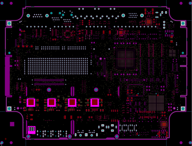
Multiple leadless parts (BGAs and QFNs) can be seen in this PCB layout.
Take Control of PCB and PCBA Pricing Early
With bare PCB pricing, you can't ever get a realistic cost for fabrication until you send the fab data to the manufacturer. Preliminary pricing is always difficult for bare PCBs. Factors like tooling cost, materials, and specialized processing (HDI or sub-laminations) all impact the PCB fabrication cost. For this reason, it is common practice to send preliminary Gerbers, such as from an old design revision or incomplete design, to get a rough estimate of per-board or per-panel PCB pricing.
However, the other two areas of electronics manufacturing, PCB assembly and component costs, can be controlled early and can be predicted easily.
PCB Assembly Pricing
At low volume or in prototyping, the cost of PCB assembly can be compared with many quick-turn shops as they provide cost estimate tools on their websites. These estimate tools typically require you to input several pieces of information about your assembly:
- Number of PCBs to be assembled
- Total part count in the BOM
- Total number of BOM lines (i.e., number of unique parts)
- Single-sided or double-sided assembly
- Number of through-hole parts
- Number of leadless parts (BGAs, QFNs, LGAs, DFNs, etc.)
- Whether the design contains small SMD packages (0201, 01005, etc.)
Based on the desired lead time and service level, the cost can be estimated by the vendor. If one of these tools is unavailable with your assembly vendor, you can send a request to the assembler with the above information. Some companies will give you a budgetary quote for the assembly work.
At high volume, the per-board assembly cost will need to be evaluated carefully from a thorough review of the design. In prototyping, the built-in margin is typically enough to cover inspection, rework, tooling, and potential rework. At high volume, much more design detail is needed from a review before providing a firm PCBA quote.
PCB Component Cost
Component costs can also be determined quite accurately as long as the schematics and BOM are finalized. The BOM cost is determined by creating a dummy component order on a distributor’s webpage or quote form.
Make sure to include the vendor’s attrition requirements as you’ll need these to estimate component costs!
The simplest way to get component costs is to start uploading a copy of your BOM into distributor websites to get a quote. Distributors are where you’ll end up purchasing the parts for consigned assembly, so they are the natural place to start looking for parts pricing. However, you will normally need more than one distributor to cover your BOM, and searching through multiple distributor sites takes time. The tools inside your ECAD software and PDM can help you quickly build PCBA pricing estimates from your BOM.
ActiveBOM in Altium Designer
ActiveBOM takes your BOM and extracts pricing information based on the distributors chosen for your parts in your parts library. The tool allows you to build a BOM inside Altium Designer without exporting Excel sheets and uploading them to distributor websites. Instead, distributor information is taken directly out of your PCB project and/or your libraries and supply information is pulled into the ActiveBOM utility directly.

BOM Tool in Octopart
For PCB designers who do not use Altium Designer, the BOM Tool in Octopart is a free utility for costing and managing a BOM. Users can upload a BOM and build a component cost estimate across their preferred vendors in an online tool that automatically pulls supply chain data for each line item in the BOM. The utility then provides an estimate for your entire BOM across all your preferred parts vendors.
BOM Portal in Altium 365
The BOM Portal in Altium 365 brings supply chain management capabilities into your PCB PDM platform. It provides the same costing features found in Octopart’s free BOM Tool and integrates with additional data sources for immediate obsolescence management, alternates selection, and compliance. By pulling data directly from your PCB design data, it functions as the primary supply chain management dashboard for a PCB project.

Service Level
Finally, the service level you expect to receive will determine the pricing costs in PCBA production. Specialized testing, on-the-line programming or firmware flashing, and special packaging all count as special service levels that carry additional costs. Different manufacturers will offer different levels of expertise in these areas, and this will impact the PCBA pricing.
The most common impact on assembly and components cost is turnkey service. In this service level, the manufacturer sources all parts (including attrition) and handles as many of the engineering/service questions as possible. The alternative is consigned assembly, where the buyer sources the parts themselves and ships these to the assembler. Turnkey always includes a markup on the component costs, which can be advantageous in offsetting shipping and import duties in consigned assembly.
Whether you need to build reliable power electronics or advanced digital systems, use Altium’s complete set of PCB design features and world-class CAD tools. Altium provides the world’s premier electronic product development platform, complete with the industry’s best PCB design tools and cross-disciplinary collaboration features for advanced design teams. Contact an expert at Altium today!


