Pi.MX8 Project – Introduction and Overview

Chapters
1
Introduction and Overview
| Created: January 18, 20242
3
4
5
PCB Assembly (and Testing)
| Coming soonThe Raspberry Pi company has developed what is probably the most popular and widely used single board computer on the market. These powerful single-board computers have long been used not only in the maker and hobbyist scene, but also in the industrial space.
As the application area expands, the form factor of these boards is emerging as a 'de facto' standard for single board computers and modules. The introduction of the compute module CM4 in late 2020 marked the establishment of a new form factor standard for system-on-modules.
Since then, various SoCs from manufacturers like Allwinner and Rockchip, along with robust FPGAs, have seamlessly integrated into the widely adopted CM4 form factor.
Motivation
The Pi.MX8 module will join the list of CM4 compatible modules.
With all this variety of compatible SoMs available, why should we invest time in designing yet another variant?
The answer is simple: when we build a complex and sometimes costly system around a computer module, we also want to have design sovereignty over the module itself. We want to have access to the schematic and layout source data, we want to be able to decide on the BOM of the module ourselves in case of component shortages, and most importantly, we want to have access to the documentation of all components used on the PCB.
All of this is only possible in the context of a fully open-source project, utilizing components with readily available documentation.

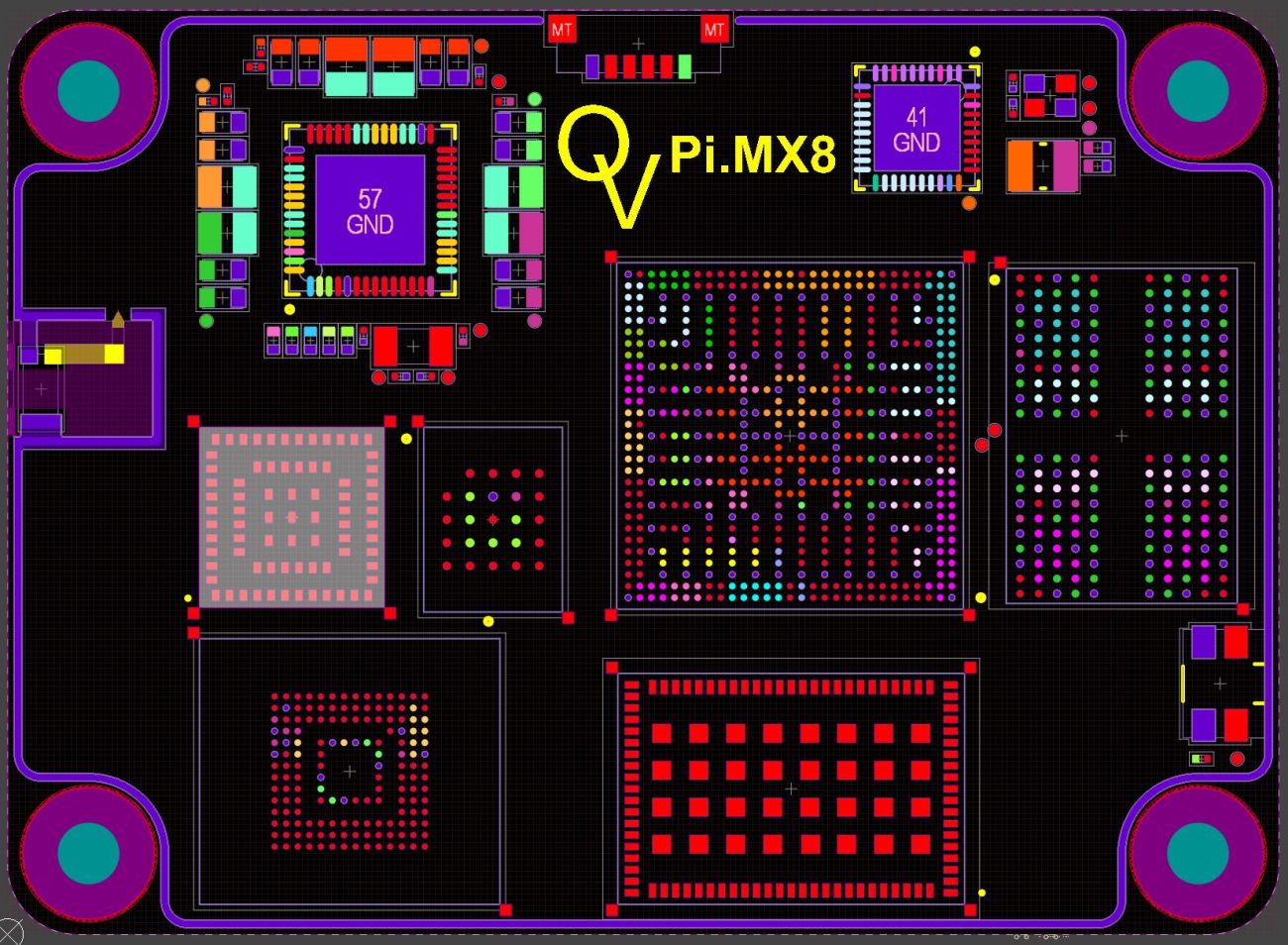
Image of the previous Pi.MX8 layout revision
In this and the following articles we will be looking into designing a fully open-source CM4 compatible module. At the end of our journey the source data for the CM4 compatible module will be published for anyone to review, modify, or build upon!
Selecting the main SoC
The core building block we must define before choosing any of the peripheral components is the System-on-Chip. There is a SoC that meets all the requirements for easily accessible documentation and is widely used in the industry, the i.MX8M Plus from NXP.
This SoC is available in several variants, ranging from two to four Cortex-A53 cores clocked at up to 1.8 GHz. Additionally, a secondary cortex M7 core and an integrated machine learning accelerator is available within this processor series.

i.MX8M Plus SoC hardware features - image source: NXP Website
The i.MX8 provides almost all the peripheral interfaces as the BCM2711 used on the Raspberry Pi CM4 module with one major exception:
Only one HDMI interface is available on the i.MX8 compared to two ports available on the BCM2711. This limitation could be bypassed by using a DSI to HDMI bridge. To keep the part count and complexity low this IC won´t be integrated on our module for now.
Other than the second HDMI interface the i.MX8 is a great fit for our application!
Peripheral components
The module's high level block diagram consists of just a few key components. The central building block is the i.MX8 SoC which provides all the interfaces for the necessary peripheral components. Simply put, we are building a breakout board for the i.MX8 processor:
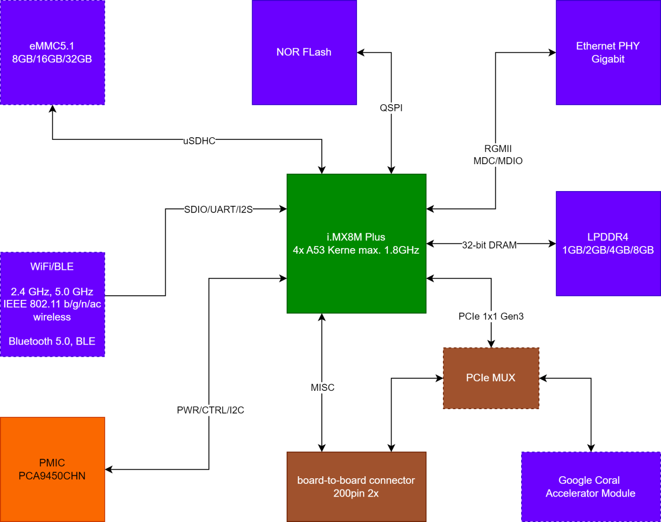
Block diagram of the Pi.MX8
PMIC
Let's start by looking at the power supply for the system. The power management IC (short PMIC) provides several voltage rails needed by the SoC, but is also designed to supply power to interfaces like the SD card connector.
The PMIC is also responsible for ensuring the correct power-up and power-down sequence, which can get quite complicated for larger SoCs.
NXP offers a PMIC that has been specially developed for use with the i.MX 8M application processors. This IC provides up to 11 voltage rails generated by a combination of buck converters and LDOs. The core voltages for the SoC are generated by buck converters as the current requirement is quite high at the low operating voltages. The voltage rail, which supplies the four A53 cores, is generated by a two-phase buck converter integrated in the PMIC to satisfy the high current demand.
The PMIC we will be using is the PCA9450.
NOR Flash
A low-capacity NOR flash can be used to store board-specific data as well as a boot medium. The i.MX8 SoC among others supports several SPI interfaces to access the boot medium. In this case, we are using a quad SPI interface to connect to a 32MB SPI NOR flash.
The device is a IS25WP256D-RHLE from Integrated Silicon Solution, Inc.
This specific package and pinout is also available from different manufacturers, making it possible to swap the component in the event of availability issues.
Ethernet PHY
The ethernet PHY needs to support gigabit speeds as well as the precision time protocol in order to be compatible with the CM4 functionality. The interface to the SoC should be a reduced gigabit media-independent interface (RGMII). This interface type is supported by a wide variety of ethernet PHYs for embedded applications.
We will be using the LAN8840 from Microchip Technology.
This PHY supports both gigabit speeds as well as high precision time stamping according to IEEE 1588- 2008 (v2). The QFN48 package is also relatively compact which saves valuable board space on the module.
DRAM
We will be using low power DDR4 memory on the Pi.MX8 module. Several manufacturers provide LPDDR4 ICs in the same package and pinout which makes it easier to react to availability issues or to support multiple memory capacities. Samsung and Micron are the most commonly used manufacturers for LPDDR4 devices. We will be using devices supporting a 32-bit wide bus at transfer speeds of 3733 Mbps.
The Pi.MX8 can be equipped with several memory capacities:

Memory Capacities Table
Coral Edge TPU
The coral edge TPU can be used to accelerate neural network computation on embedded devices. The Coral TPU is often used in the form of an M.2 expansion card, and is also available in a small LGA package.
This module contains the tensor processor as well as the power management IC necessary for operating the TPU. We need to provide a PCIe interface to this module to make use of the available processing power.
Because this module is specific to only a small number of use-cases and is relatively expensive, we will implement it as an assembly variant.
WiFi/BLE Module
WiFi and Bluetooth low energy are one of the most commonly used wireless interfaces for IoT applications. We will be using a MURATA LBEE5PK2BC module as a fully integrated solution.
This module provides both W-LAN and Bluetooth while minimizing the count of external components needed. Not every application needs wireless connectivity which is why the WiFi/BLE module will be implemented as an assembly variant as well.
eMMC storage
An eMMC module provides up to 32GB storage capacity to the Pi.MX8 module. As with the LPDDR4 DRAM we can choose between many manufacturers for the eMMC storage module that adhere to the same package and pinout standard. One of the most commonly used manufacturers for eMMC modules is SanDisk.
The eMMC will also be implemented as an assembly variant in order to save BOM cost for applications that do not have a high demand for data storage capacity.
Test fitting key components
Before moving onto the next stage of setting up the schematic and PCB design, let's take a quick look at the space requirements for all the components we´ve just selected.
For this purpose we can set up the PCB library components and place them within the PCB outline of the CM4 formfactor.
Test-fitting the key components
All of the key components fit on the top layer within the CM4 formfactor outline. This rough placement also shows that there is little space left for larger components on the top side. The mated height of the board-to-board connectors we are using is only 2mm. This restricts the height of components we can place on the bottom side of the PCB. Ideally, all the key components will be placed on the top side of the board to avoid any collisions with parts that might be placed on the carrier board underneath the module.
What's next?
Exciting updates ahead! With component selection complete, our journey continues to finalize the schematics in the upcoming update. Notice anything missing in the PCB layout screenshot at the start? That's because it's an older revision, and we're re-routing the entire PCB to incorporate the new functionality. Join us for the ride and follow the real-time progress through the embedded A365 viewer and our public workspace! Don't miss out—stay tuned for the thrilling transformation!


About Author
Related Resources


Related Technical Documentation


Take advantage of the world's
most trusted PCB design system.
One interface. One data
model. Endless possibilities.
Effortlessly collaborate with
mechanical designers.
The world's most trusted
PCB design platform
Best in class interactive
routing
View License Options
Thank you, you are now subscribed to updates.