


Pi.MX8 Project - Board Layout Part 1


Chapters
1
2
3
Board Layout Part 1
| Created: February 22, 20244
5
6
7
PCB Assembly
| Coming soonWelcome to the third installment of the Pi.MX8 open-source computer module project! In this article series, we delve into the design and testing of a system-on-module based on an i.MX8M plus processor from NXP.

In the last update, we looked at the schematic structure of the module and started preparing the preliminary component placement. Now that we’ve placed the components, we have a good idea of the density of the design and the demands this places on the layerstack. Today, we will select a suitable stackup and start routing the first tracks.
Defining the layerstack
Based on the component placement and a few strategic factors we can decide which PCB technology and which layerstack we would like to use for the design going forward. Let's take a look at the component density first:

Component placement top side
The preliminary component placement reveals a moderate overall design density. The active components are all located on the top side of the board, while the bottom side mainly contains decoupling capacitors and other passive circuitry. The bottom side of the board is therefore relatively empty and leaves us with plenty of routing space. The goal, however, would be to allocate this space for additional features that will be implemented as the Pi.MX8 module is intended to serve as a platform that can be updated and expanded upon specific requests.

Component placement bottom side
Looking at the component placement close to the board-to-board connectors we notice that many components are placed directly over the connectors on the opposite side of the board. If we decide to use only standard VIAs that connect the entire layerstack from the top to the bottom layer, we cannot place any VIAs in these areas. In order to break out all the pins on the board-to-board connectors and efficiently route the active circuitry situated on the opposite side of the connectors, we need to devise a method that goes beyond relying solely on through-hole VIAs. For this, we will need to use an HDI stackup.
Using an HDI stack makes it easier to expand the functionality of the module at a later stage, as we do not necessarily have to use through-hole VIAs to connect additional components, and therefore do not have to interfere as much with the established routing and component placement.
For the Pi.MX8 module we will be using a 2+N+2 layerstack. This is a type III layerstack as defined in the IPC-2226 standards and is one of the most commonly used HDI stacks.
This type of stackup uses two sequential lamination steps in the manufacturing process in order to allow micro-VIAs to connect the three outermost layers. A buried VIA is used to connect the core stack that is not part of the sequential manufacturing process. The prepregs and the prepreg thickness used in this type of layerstack depend on the manufacturing capability of the PCB provider. The chosen thickness of the sequential laminated prepregs is limited by the aspect ratio of the micro VIA. In contrast to mechanically drilled VIAs, micro VIAs are created by punching holes in the prepregs using short laser pulses. Typically, VIA diameters between 0.08mm and 0.15mm are used. An aspect ratio suitable for mass manufacturing usually is in the range of 0.6:1 – 0.8:1.
A thin prepreg will ensure the aspect ratio requirement is not violated while reducing the track width for a given impedance-controlled trace. For a simple microstrip on the top or bottom layer with only one reference plane this is not a problem. We have to be careful with the embedded striplines underneath the first ground plane, however, as short distances to the reference plane above and below the striplines might result in very narrow traces for certain impedance controlled interfaces.
The final stackup for the Pi.MX8 board was created in cooperation with the PCB manufacturer and looks as follows:

Pi.MX8 Layerstack
Overall, the module will be built on a 10-Layer stackup. The top, L2, L7, and bottom layers will be used as signal layers. Layer L1, L3, L6 and L8 will be used as ground planes. The two remaining layers L4 and L5 will act as the power planes. The power planes are built using a thin foil of only 18μm thickness. We have to keep an eye on the IR drop for these layers. The power planes are closely coupled to the neighboring ground planes with only a 75μm prepreg separating these layers. This results in additional plane capacitance which can be beneficial for providing a low PDN impedance at high frequencies. We´ll verify the PDN behavior by simulation once we have the layout completed.
Another important aspect to note about this stackup is that we will be using only staggered instead of stacked micro VIAs. This means that micro VIAs can´t be placed directly on top of each other and instead must be offset with a pitch of at least 0.35mm center to center. Using staggered VIAs makes the registration of the sequential layers easier which decreases manufacturing cost with some PCB providers. This approach is also recommended for HDI stackups using more than two micro VIA programs to increase the reliability of the micro VIAs. The drawback of using staggered micro VIAs is the additional space needed to meet the minimum offset requirement. The voids created in the ground plane also need to be considered when it comes to managing the return path for neighboring traces.
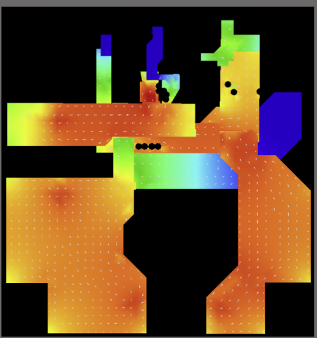
Component break-out routing
Now that the layer stack has been defined, the next step is to break out the signals of the individual components. In this step, we’re going to place all the necessary VIAs for signal and power routing on each component. We do this step now since we’d ideally like to have all VIAs in place before we start to connect the components. Even in a HDI stackup, VIAs still take up a lot of space. This is especially true for VIAs that are part of the power distribution network as they usually connect through the whole stackup. Placing VIAs during the routing stage may require previously routed traces to be deleted to make room for VIAs.

Break-out routing on the top layer of the module
In the image above we can see that almost all component pins are broken out using VIAs or are left unconnected. The unconnected pads will be routed on the top layer or are provided with additional space to add the break-out routing later on. In the latter case, it's important to remember not to place any traces within those areas.
For some components, it will be necessary to locally override the predefined design rules for trace width and spacing to make the break-out routing possible. One such example is the i.MX8 SoC. The small pin pitch of only 0.5mm requires a trace width of 0.08mm and a trace to pad spacing of 0.085mm. Outside of these break-out areas we'd like to continue working with 100um trace width and spacing rules. There are several ways to implement this behavior in the design rules. One way is by using extra design rooms that are assigned a dedicated set of rules. This enables a smooth routing workflow as the trace width gets automatically adjusted once the cursor crosses the border of the design room.

Trace width and spacing requirements for the i.MX8 break-out routing
By using design rooms the trace width gets automatically adjusted during interactive routing:
{"preview_thumbnail":"/sites/default/files/styles/video_embed_wysiwyg_preview/public/video_thumbnails/4Xt_JHUyDKs.jpg?itok=qUoPCb7m","video_url":"https://youtu.be/4Xt_JHUyDKs","settings":{"responsive":1,"width":"854","height":"480","autoplay":1,"title_format":"@provider | @title","title_fallback":true,"loading":"lazy"},"settings_summary":["Embedded Video (Responsive, autoplaying)."]}
In our next update, we’ll explore how general design rules are set up according to the layerstack impedance profile, as well as how to approach the routing on the inner layers. Stay tuned to find out how we address the memory layout and navigate the difficulties introduced by the chosen HDI stackup!

About Author
Related Resources
Related Technical Documentation
Design to Release, Without the Friction
- Keep reviews tied to the right version
- Reduce handoff confusion and rework
- Spot sourcing and release risk earlier
- Work solo, share when needed
Get Started
Thank you, you are now subscribed to updates.

