


Dual ADC Module PCB Design Project

At a Glance
ADCs in a PCB are examined in this project, including placement and routing involving an isolated ADC.


Click here to jump to the viewer embed and browse this project
If your board includes an ADC, then your board qualifies as a mixed-signal system and it will need some particular layout practices to prevent excess noise on analog lines. ADCs are normally non-isolated components, but they also come in an isolated variety, where the component provides galvanic isolation between the analog and digital sides.
In this project, I’m going to show an example design that uses both types of ADCs in the same PCB layout. These components require different layout practices, but we’ll implement them on the same board to provide a good comparison.
As is the case in all our projects, there is a link to download the source files for this project at the end of the article. To learn more about using these types of components and to follow along with the entire layout process, you can watch the playlist below.
Starting the ADC Module
The ADC module I’ll present in this project is intended to collect two signals and pass the data to a pin header, which could then connect to an external board like a microcontroller module. The module will include the following set of major components:
- ISL75051ASEHVFE - Rad-hard 5V to 3V3 power regulator module
- ADC128S102CIMTX - 8-Channel, 0.5 to 1 MSps 12-bit ADC
- AMC1203BPSA - Single-channel 40 kSps 8-bit sigma-delta isolated current-sensing ADC
The signals being collected are intended to be at low frequencies, as evidenced by their low sample rates. Both ADCs assume low-impedance sources, so we do not need an active filter with an impedance buffer, and we can connect directly to the ADC inputs if desired. Finally, anyone familiar with Intersil components will note that the ISL75051ASEHVFE is a rad-hard regulator; this module could be used in a space system as long as the other two components can be aerospace qualified.
Schematics of Isolated and Non-Isolated ADCs
The images below show the two main portions of the schematics for this module: the isolated and non-isolated ADCs. The remaining components and circuits can be seen in the project files.
The schematics are simple; we only have one page needed for all the circuits. We have two separate power inputs, one for the isolated side coming through an SMA, and another for the non-isolated side coming through the pin header.
First, take a look at the schematics for the isolated ADC (AMC1203BPSA) as shown below.

The analog reference for this component is set internally, so we do not need a precision reference chip to set the measurement range. Note that the isolated ADC requires two different power nets (+5V and +5V_AN), both at +5V based on the datasheet; these must come from different supplies in order to ensure galvanic isolation is maintained across the isolation gap in this component. J1 and J3 are the connectors for the incoming analog signal and the input power for the analog side of the ADC.
To properly shield the incoming signals, the signals coming to the isolated and non-isolated ADCs are provided using coaxial cable with vertical SMA connectors (73251-1350 from Molex). These connectors and the attached coaxial cables will have 50 Ohms impedance, but the input signals will be low enough that the only appreciable interaction exists between the source and the load in the system.
Next, take a look at the circuit for the standard ADC.

In this circuit, power is provided by the regulator (3V3 net), which in turn receives its power from the +5V connection from the pin header. The SPI output uses a resistor to slow down the edge rate slightly before routing the signal off-board. Capacitors are also placed for specifically decoupling/bypassing the VA and VD pins.
There are some assumptions in the above schematics:
- The +5V_AN net will never need high current in this board, thus using an SMA + coax cable for power is appropriate. Higher voltages/currents over this will require different components.
- The input signal bandwidth is only limited by the sampling rate of each ADC. If lower bandwidth is needed, add a low-pass RC filter and run at maximum sample rate for anti-aliasing.
- The +5V connection on the pin header is assumed to be regulated and relatively noise-free. If unregulated, a +5V regulator will be needed on the input.
- The VA and VD pins on U2 are not isolated because U2 is the only component pulling fast digital edges for its SPI interface. If there were more components on the 3V3 bus, then we would definitely want to consider band-limiting power to the VA pin near 1 MHz.
With these points out of the way, we can proceed to the stackup. Our stackup will need to support 2 reasonably fast digital interfaces (one for each ADC) and two separate feedlines into the ADCs.
Floorplanning and PCB Stackup
Because this board contains an isolated component, the board needs to have a particular floor plan that enables an isolated region. We can do everything in this board on a single layer, but we need ground in order to prevent inductive coupling between analog and digital sections, which demands an internal ground plane. Therefore, we can use a simple 4-layer PCB stackup with internal GND.
The finalized stackup is shown below. In this stackup, we have used a SIG+PWR/GND/GND/SIG stackup; components will be on the top side and the bottom side can be used for additional routing as needed.
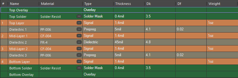
In this stackup, the Dk value is not so important as we do not have controlled impedance requirements. The important point here is the thin outer layer, as well as GND on L2 and L3. The thin outer layer with adjacent ground is key to suppressing noise, as I’ve pointed out in a different article on parasitic extraction.
Next, the isolated section needs to be placed in its own area with its SMA connectors providing power and signal. I’ve isolated this into the left side of the board, while the remaining components will sit on the right side. The initial placement is shown below.

The initial placement lines all the analog sections up on the left side of the board, while the regulator and I/O lines are routed directly away to the right (primarily on the back layer). This is a typical strategy for minimizing noise coupling between the digital lines and the analog feedlines. The isolation barrier runs vertically under U3, so that is where we will split out ground nets into GND and AGND to maintain the required isolation.
To do this split, I’ve implemented a small copper pour region that spans through all 4 layers in the PCB. The region provides AGND connections on J1 and J3, and the layers will be connected with stitching vias.

The thermal connections on the SMA pads will be removed by changing the design rules. I use a similar strategy in the non-isolated section, but with the difference being that the pour on L2 runs under the entire ADC connection. I’ll also add stitching vias to that section for noise suppression. With this point completed, we can now route the rest of the connections.
One point I would like to note here is the capacitor placement. Just as is the case with a digital component, it's important to place any caps that supply power to the analog power pin close to those pins. This way, the analog subsystem will be able to draw sufficient power within its sampling interval and there will be minimal dropout for any internal reference. An example is shown below. Specifically, we have placed C18 and C19 for the digital supply, and C16 and C17 for the analog side.

Finalized Routing and Layout
After some component shifts, I was able to move the large capacitors (C9 and C13) so that they sit more in the center of the board. This allows me to reduce the board size somewhat so that we do not have a big open area with no components or routing. Then on L2 and L3, I have run ground everywhere to keep the copper distribution in the stackup mostly symmetric. The finalized routing, with stitching vias included, is shown below.

In this view, you can see the +5V input and +3V3 output routed as large polygons, while the other polygons on the top layer are GND or AGND. All digital signals are routed on the bottom layer except for points where they need to connect to the ADCs on L1.
A 3D view of the finalized PCB layout is shown in the image below. As usual, we have some logos, as well as a silkscreen legend for the pinout on the pin header. The SMAs placed on the left side have stitching vias to tie that ground region together on all layers and to prevent stray RF interference from propagating into that portion of the substrate. These lines are also not designed to a specific impedance, and the assumption here is that the input signals will be of such low frequencies that feedlines are electrically short.

What Else Can We Add to This Module?
The design as shown above is intended to interface with an external microcontroller module to collect and process the data via the pin header. To continue developing this board, one could place a digital section with a microcontroller on the back layer, where the microcontroller accepts data provided by the outputs from the ADCs. A small microcontroller like PIC (from Microchip) or a smaller STM32 (ST Microelectronics) would be appropriate for this module.
The design as it sits now assumes a low source impedance and no filtering to limit the bandwidth of the signal being collected by the device. This is already limited by the sample rate based on the Nyquist sampling rate, but low-frequency signals could be oversampled and fed through an RC anti-aliasing filter to further reduce noise.
If you use a microcontroller on the back layer, it will likely have its output interface to send data to another device, such as a computer. This could be done over a UART interface, or directly over USB. The UART option is useful as it could then be routed to a 2-pin header, which then would be connected to the destination device. Because so many microcontrollers have a UART option, the next project I’ll present will be a UART to USB converter module that could accept data from a microcontroller as I’ve described here.
Follow this link to download a ZIP archive with the project source files. You can also use the download link in the above embed to access the source files.
High-density components with RF sections are easy to place and route with the complete set of CAD utilities in Altium Designer®. When you’ve finished your design, and you want to release files to your manufacturer, the Altium 365™ platform makes it easy to collaborate and share your projects.
We have only scratched the surface of what’s possible with Altium Designer on Altium 365. Start your free trial of Altium Designer + Altium 365 today.

About Author
Related Resources
Related Technical Documentation
Table of Contents
Design to Release, Without the Friction
- Keep reviews tied to the right version
- Reduce handoff confusion and rework
- Spot sourcing and release risk earlier
- Work solo, share when needed
Get Started
Thank you, you are now subscribed to updates.

