


RF Power Amplifier Module PCB Design

At a Glance
We’ll examine how to design a PCB with a power amplifier. This module generates its own source signal using a VCO.


Click here to jump to the viewer embed and browse this project
RF power amplifiers can be found in any wireless product, often built into chipsets or modems. However, in some specialty systems, you might need higher power output at a specific frequency, and this requires a discrete amplifier circuit to provide that power. These systems can take an external oscillator and amplify it to provide a high power signal, or a local oscillator can be used to generate the required signal that will be fed into the amplifier.
In this example project, I’m going to show how to design a power amplifier module that operates in the 6 GHz range with high power output (above approximately 10 dB). The module I’ll show here provides high power output by amplifying the signal with +13 dB gain, and the signal is passed to an SMA connector. The module is meant to be entirely self-contained; simply apply power and you get a high-frequency signal at the output port!
Watch the playlist below to learn more about power amplifier design and layout for systems operating in the 6 GHz range.
Our Power Amplifier PCB Module
The power amplifier component we will use in this example is the HMC637ALP5E from Hittite Microwave (now Analog Devices). This part has very high gain and saturation levels (in terms of IP3 point and -1 dB compression), as well as low return loss and simple layout requirements. The design is in a QFN package, but most of the pins are ground or NC.
The signal source in this design will be a voltage-controlled oscillator (VCO). These components are also very simple to work with in schematics and circuits. For a PCB layout, they do require some important considerations on impedance control and isolation, but the output can be fed directly to the power amplifier. Given the power output of this VCO, the amplifier will be operating very solidly in the linear range, so we would expect minimal harmonic generation.
In addition, we will have two important power circuits and some ancillary components:
Power Amp Circuit
The power amplifier in this example module requires two gate voltages and a primary drain voltage for power. The response range is very broad, from DC to about 6 GHz. The power amplifier’s response range is listed as 6 GHz maximum in the datasheet, but if you look at all of the graphs from page 2 to 3 in the datasheet, you’ll see that the response is consistent all the way out to approximately 8 GHz. Therefore, we can most likely run slightly above 6 GHz and the system will work fine.
The power amplifier circuit in the schematics is shown below. We have AC coupling on the RFIN and RFOUT lines as specified in the datasheets for our components.

The gate voltages being applied to the amplifier are provided through a set of pin headers on the PCB. The idea here is to be able to disconnect one of the headers and connect to an external bench power supply if needed. This also allows the power-up sequence for the amplifier to be applied manually. See page of the HMC637ALP5E datasheet for the power-up procedure.
VCO, Amplifier Response, and its Tuning Voltage
The VCO on this board is part number HMC358MS8GE. This component has very simple usage and the output can be adjusted with a DC tuning voltage applied at the VTUNE pin. The output ranges from 5.8 GHz to 6.8 GHz. The VCO circuit is shown below.

The 3 V power connection to this VCO on the VTUNE pin causes the oscillator to produce a 6.3 GHz signal at the output pin. Note that, from the HMC637ALP5E datasheet, that we can expect consistent response from the amplifier at 6.3 GHz despite the stated cutoff of 6 GHz. Therefore, in the initial revision of this design, we’ll stick with the direct 3V connection to VTUNE. At the end of the article, I’ve outlined a few ways that the tuning voltage could be made adjustable.
Bias Tee
The VDD power is given to the power amplifier using a bias tee circuit. A bias tee that only uses a single capacitor and inductor can be easily designed to meet two requirements:
- There will be some minimum required capacitance needed to pass the AC signal
- There will be some impedance ratio between the DC path and the AC path that determines the level of isolation on the DC source
- The inductance will need to be larger when higher isolation impedance is required on the DC side
The bias tee circuit I’ve used is shown below.

At the VCO output of 6.3 GHz, this bias tee will have an impedance ratio of approximately 43:1. In the past, I have used another power amplifier with a bias tee that can operate just fine with as low as a 1:1 impedance ratio. However, because this bias tee connects back to a pin header, I would worry about some of the signal radiating strongly off one of the pins. Therefore, if your goal is maximum power transfer through to the load, you might find that the capacitor needs to be decreased or the inductor needs to be increased, but this may alter the passband of the bias tee. The bias tee bandwidth/passband should be checked for DC blocking and power delivery at the amplifier's operating frequency.
I've covered the specifics of bias tee design in a different article, in this article I cover simulations of this bias tee and show the power delivery with the current bias tee, as well as an optimized bias tee that provides maximum power delivery to a 50 Ohm load.
Stackup and PCB Layout
This board will be placed on a 4-layer stackup with coplanar routing for the RF lines. Using a 4-layer stackup allows me to put ground below the surface layer. This board will have all the required components placed on the top layer of the PCB, as well as the RF interconnect routing. The bottom layer can be used for routing power rails, and the inner layers will be GND. This type of stackup and routing will ensure maximum isolation between the RF section and the power regulator section through parasitic reduction.

The material system being used here is a low-Dk FR4; example brand names that could meet this spec are Isola 370HR or ITEQ. Note that for this type of design, where the interconnect length is somewhat short, there will not be excessive losses and we do not need a low-loss material like Rogers.
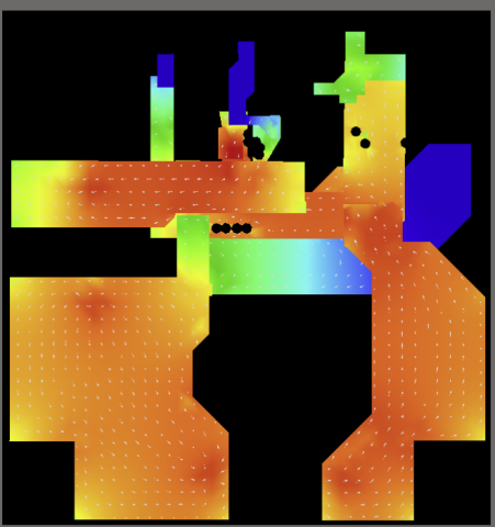
The PCB layout for this module requires segmentation between the power circuits and the RF circuits. In particular, the main 12V to 5V switching regulator will take up a decent amount of space. With the small board size, any switching elements should be kept away from the RF lines in the initial floor plan for this board. The initial regions where I’ll apply placement are shown below.

The floorplan above does three things:
- By taking advantage of ground on L2, we have excellent noise control around the power regulators
- It leaves enough room around the RF lines and the components for the pin headers
- It leaves a straight-line path from the VCO to the amplifier and the output SMA connector (J1)
Placement and layout for the power regulator circuits is elementary, so I won’t repeat it in this article. You can read more about best practices for power supply layout and switching regulator layout at this link.
The RF routing section is shown below. The impedance profile shown in the stackup above was used as the design rule for the RF nets; this setting is outlined in the video linked above. I added shielding to the RF nets so that the 6 GHz signal can be contained along the interconnect with minimal leakage. The spacing between these vias is a bit aggressive; the hole wall-to-hole wall spacing is only 12 mil, which is close to the typical minimum of 8 or 10 mil that would typically be specified by a fabrication house.

The finished layout is shown below. Stitching vias were added with high-frequency cutoff to prevent switching noise from resonating in the top layer. Finally, I added some silkscreen with logos and voltage indicators on the pin headers to assist in the power-up procedure.

How to Improve This Design
This design operates at a fixed frequency being output into a wideband amplifier. If we wanted to, we could modify the design to include a tunable output voltage by implementing capability to adjust the voltage at the VTUNE pin. Some other improvements may be appropriate after testing. There are several options:
- If needed, the bias tee inductor could be swapped for a 10x-100x larger value to increase the impedance ratio at the output, but be careful of the effect on the desired bandwidth.
- Use a potentiometer in a voltage divider across the VTUNE pin.
- Use a DAC or adjustable regulator to adjust the voltage on the VTUNE pin; this would require an additional pin header to an external MCU module (like our nRF52 module).
- Add a pin header so that an external voltage source could be used for tuning.
- Consider adding a taper into/out of larger pads on C6 and the SMA connectors for smooth transitions; on the SMAs there could be a slight mismatch that would require a taper to compensate.
- Continuing on point #5, perform a simulation for the CPW with the via fence to ensure the impedance target is hit.
- While the SMAs will work with a small gap to the bottom pins, thickening up the board is preferrable; a manufacturer could provide a stackup that will do this.
This might be very useful if, for example, you wanted to bring the output signal back into the power amp’s rated maximum frequency of 6 GHz. As I mentioned above, you could also simply ground the VTUNE pin to permanently set the VCO’s output to 5.8 GHz.
Finally, to access an antenna, we could add a patch antenna on the back layer and add a probe-coupled connection to the antenna through a via. It would be quite simple to place a via to a probe-fed patch antenna on the back side of the board. However, due to the power routing on the back layer, the easiest way to accomplish this is to change the stackup to a 6-layer PCB.
Follow this link to download a ZIP archive with the project source files. You can also use the download link in the above embed to access the source files.
Whenever you need to create complex RF systems with a power amplifier or VCO, use the 2D and 3D CAD tools in Altium. When you’ve finished your design, and you want to release files to your manufacturer, Altium makes it easy to collaborate and share your projects.

About Author
Related Resources
Related Technical Documentation
Table of Contents
Design to Release, Without the Friction
- Keep reviews tied to the right version
- Reduce handoff confusion and rework
- Spot sourcing and release risk earlier
- Work solo, share when needed
Get Started
Thank you, you are now subscribed to updates.

