Pi.MX8 Project – Schematic Structure and Component Placement

Chapters
1
2
Component Placement and Layout Planning
| Created: February 06, 20243
4
5
PCB Assembly (and Testing)
| Coming soonWelcome to the second installment of the Pi.MX8 open-source compute module project! In this article series, we delve into the design and testing of a system-on-module based on an i.MX8M plus processor from NXP.
In the previous update, we discussed the motivation behind this project as well as which features our module should have and which components we would like to use to implement them.
This time, we will like to focus on the structure of the schematic design and how we can get started with the PCB layout.
Schematic structure
Let's start by looking at how the schematic is organized. Two approaches are typically used for handling the schematic capture; flat and hierarchical designs.
A flat schematic can best be pictured as a large single page schematic which is simply divided into several sheets. Connections between the sheets can be established using off-sheet connectors for example.
In a hierarchical circuit diagram, the design can be divided into function blocks that are represented as sheet symbols, which in turn can be interconnected or even nested. This approach is often used in large designs as it allows you to more effectively break down a large schematic into blocks that can be designed and viewed independently from each other. The connections between these functional blocks are established using ports which will be represented on the sheet symbol. With the exception of power objects (VCC, GND etc.) only ports are used to link the schematic sheets together.
The Pi.MX8 schematic uses this hierarchical topology:

The design is divided into several functional blocks—all represented in one top-level sheet. Here, all the connections between the separate sheets are established. This design uses only one hierarchical level.
The iMX8 SoC is divided into several parts which are placed on multiple sheets. On the top-level sheet, the large symbol in the center of the page represents the SoC. The two large sheet symbols on the left and right side of the page represent the two board-to-board connectors of the Pi.MX8 module. All other functional blocks are represented with their own sheet symbol.
Each page follows the same design philosophy. Interfaces leaving a schematic page are color coded to represent the voltage level of the interface. Nets that are part of the power distribution network are drawn with a thick linewidth.
Integrating notes for specific configuration settings, naming conventions or general remarks can be used to speed up the debugging and bring-up process, while acting as a reminder for the PCB routing process.
Schematic page including notes and color coding
Adding notes to an Altium Designer schematic from an Excel spreadsheet or from screenshots taken from a datasheet is as easy as Ctrl+C, Ctrl+V:
The circuit diagram itself is currently still subject to changes and is therefore still under development. We will delve deeper into the schematic in a further update.
While the schematic will experience some minor changes in the next few weeks we can already go ahead and plan the PCB layout.
PCB layout planning
In the layout planning phase, we would like to define the layerstack and plan out a strategy on how to route the board. As a first step to define a layerstack and a routing approach we can place key components on the board. This will help us to estimate the space requirements and routing density which are both important factors to consider for defining a layerstack and routing strategy. Key components in this context are parts that have a large impact on the component placement which is the case for the following examples:
-
Parts with a predefined position on the PCB i.e. connectors, indicator LEDs, SMD standoffs;
-
Parts with a lot of nets that need to be routed i.e. SoCs, memory devices, MCUs;
-
Parts that occupy a lot of board space i.e. large inductors, switches, heatsinks.
Preparing the board space
Before placing any components on the Pi.MX8 module, the first thing we would like to do is define a few boundary conditions. In the context of the module these are mechanical features and dimensions dictated by the module formfactor that we would like to use.
Depending on a list of MCAD tools used we integrate with, this information can be passed into the PCB layout editor using the MCAD CoDesigner. In our case, we will import a DXF file that was created using Spaceclaim Engineer. This DXF contour is imported and placed into a new mechanical layer called “Reference”:

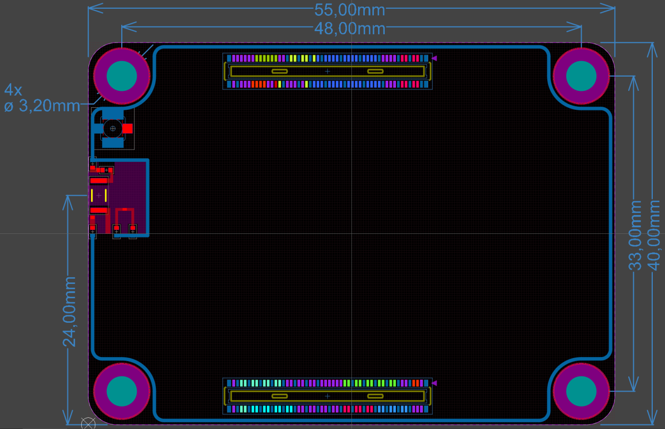
Mechanical dimensions and connector locations of the PCB
With the contour in place, we can add the mounting holes at the correct locations using the snap options in the PCB editor. The board-to-board connectors can be placed on the bottom layer of the module in the same way:

Positioning of mounting holes and connectors on the PCB
On the top layer, a U.FL connector for an external antenna is placed below the upper left mounting hole. Below the connector a chip antenna for WiFi and Bluetooth operation is placed. The position of this on-board antenna should not be changed as many already existing baseboards use a copper keepout region underneath the antenna location.
The antenna is a library component that includes not only the chip antenna itself, but also some copper geometry and reference points where matching components need to be placed. This information can be found in the antenna datasheet. By embedding this information into the library component we make sure that the pre-defined geometry doesn't accidentally get changed.

Defining the antenna location
At this stage of defining the board space that is available for routing and component placement it can also make sense to add in a guard ring along the edge of the PCB. A guard ring is a copper track that runs along the edge of the PCB on all layers and is connected to ground at regular intervals using VIAs. A guard ring placed along the edge of the board will prevent radiated emissions from the internal layers to the environment. Guard rings are also used in other configurations on a PCB, for example for precision analog electronics where leakage currents flowing through surface contaminations need to be kept out of areas with highly sensitive high impedance nodes. If such features are required these should also be considered during the layout planning phase.
Placing a guard ring along the edge of the board at this early design stage is important because while it might not seem difficult to add this feature later on, a guard ring can take up a significant amount of space. Typically the copper geometry needs to have a minimum distance of 0.2mm – 0.3mm to the machined board edge. Add to that the guard ring trace width of 0.6mm for example and another 0.1mm for the distance of the guard ring to the remaining copper traces and the board suddenly gets 2mm smaller in each direction. Especially if connectors are placed close to the board edge or if the component density on the board is very high this can make a large difference during routing.
PCB with guard ring
Another limitation we should consider for component placement is the fact that certain components may be susceptible to mechanical stress. Depending on the mounting situation of a PCB inside an enclosure, certain areas of a board can experience significant mechanical stress. Typical examples of such scenarios are mounting holes or heatsinks that apply an external mounting pressure to a PCB.
That is also something we should keep in mind for the Pi.MX8 module. The module will be mounted inside an aluminum enclosure using the four mounting holes. In this configuration, the circuit board and the housing are rigidly connected to each other. Since aluminum has a different thermal expansion coefficient than the FR4 the board starts to warp as soon as the system heats up. The magnitude of this effect depends on the exact material characteristics involved and the temperature difference seen by the assembly.
We can simulate the thermal expansion of the module mounted inside the aluminum enclosure. By calculating the gradient of the displacement vector, we can see that the board will experience movement, especially close to the mounting holes:
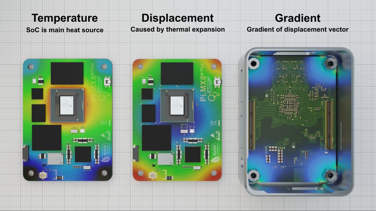
Mechanical stress caused by thermal expansion
If the PCB is used in a high vibration environment the same principle applies in regard to high stresses close to the mounting holes.
But, why is this important for the Pi.MX8 module? There are components on the module that are sensitive to external mechanical stress. These components are large ceramic capacitors. These capacitors can easily crack if they are subject to mechanical stress. Often the capacitors fail with a short circuit causing a catastrophic failure of the whole system. For this reason, large ceramic capacitors should not be placed close to mounting holes or V-cut board edges. The latter experiences high mechanical stress as well during panel separation. The larger the capacitor, the more sensitive it is to mechanical loads in the PCB.
For us that means keeping ceramic capacitors larger than 0603 that do not use soft termination at least 3.5mm from the mounting holes. This figure varies depending on the mounting situation of the board and was derived from the simulation for the Pi.MX8 board.
Keeping this in mind, the preliminary placement for the key-components on the Pi.MX8 board is as follows:

Preliminary placement of the key components
The idea behind this component placement and how it impacts the layerstack choice will be part of the next update. Stay tuned to follow along with the progress of the Pi.MX8 module!

About Author
Related Resources


Related Technical Documentation


Take advantage of the world's
most trusted PCB design system.
One interface. One data
model. Endless possibilities.
Effortlessly collaborate with
mechanical designers.
The world's most trusted
PCB design platform
Best in class interactive
routing
View License Options
Thank you, you are now subscribed to updates.