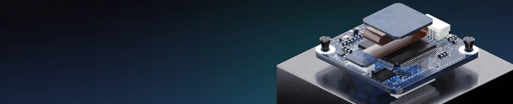
Printed Circuit Assembly and Design for Cost


The design process for an electronic system requires decisions that will influence the cost and performance of the printed circuit assembly (PCA).
General Principles
There is value in being able to quickly estimate the impact of design on cost. Because of the increasing pressure to shorten time to market, design engineers may not have the luxury of using trial and error and price quotes to fine-tune a new design. In addition, the further down the development cycle for a new product, the greater the difficulty in introducing a design change for any reason. Decisions made during the early phases of product planning and logical design have a greater impact on final cost than is often realized.
When engineers and designers understand what contributes to the cost of the printed circuit board (PCB) or PCA, and how their decisions can optimize both performance and cost, they not only save money for the immediate purchase order, but also over the entire life of the product.
Pricing Models
PCB fabricators and PCA assemblers are in business to make money, and they expect to recover their expense with at least some profit. While many elements contribute to those expenses, designers, engineers, and supply chain management professionals are most interested in the things they can directly control through their own design choices.
The operating cost of any manufacturing facility will include overhead for such things as administration and sales and marketing. However, these are usually considered design independent and outside the control of the customer. Similarly, the mark-up for profit depends less on the design, and more on how badly the supplier wants to win this business, the competitive environment, and other strategic considerations.
Design-dependent costs can be estimated by looking at the cost of the materials used in production plus the allocated cost of any processes that are used, adjusted for any yield losses that are incurred due to failures during inspection or testing. Figure 1 shows some of the cost factors.
Figure 1: The various factors that go into a pricing model for a fabricator.
The materials used to construct a PCB are the source of the direct material cost. This includes copper foil, prepreg, copper clad core laminate, and solder mask. The material cost can be easily determined from board area and details about the board construction, such as laminate type, number of layers, and number of prepreg plies. It also includes any deposited metal layer, although apart from gold this cost is negligible. For a PCA this would certainly include any attached components in the bill of materials.
Manufacturing processes are characterized by variable costs that depend on the number of units that are produced, and fixed costs that do not. Variable costs include indirect consumables, labor, and maintenance. Fixed costs. such as depreciation on capital equipment, are incurred regardless of whether the process is used. From the standpoint of design-dependent costs these can be lumped together as the total process cost.
The specific cost model for PCB or PCA suppliers can vary, however, many operations use the concept of a cost center with a specific allocation applied to each unit that passes through the center.
The internal, first-pass yield at a supplier must also be factored into the cost for several reasons. PCBs are difficult to rework, and because of the risk to long-term reliability many customers prefer suppliers scrap any boards that fail testing.
Rather than calculate a bottoms-up cost for each new design, PCB fabricators typically create a standard pricing matrix that provides a basis for quoting. This matrix assumes a standard set of design characteristics that includes laminate material, outerlayer surface finish, minimum conductor width, minimum hole size, and uses these standards to estimate the cost for a given board size and layer count. Any characteristics of the board design that deviate from standard materials and processing adds cost and is accounted for as a price adder or its own pricing model. PCA assemblers use the component bill-of-materials and a similar matrix for quoting purposes.
While each factory or supplier may have their own internal and confidential cost model, we can infer the relative cost contributions of different design features from average market price data. Figure 2 shows the results of a survey of Chinese PCB suppliers taken in July 2016 with a range of prices (in cents per square inch) for PCBs with different layer counts. Where absolute price data are unavailable, it is still possible to compare design options using a ratio, or relative price compared to a standard.
Material Cost Drivers
For PCBs the predominant driver of material cost is the dielectric laminate, including copper-clad core and prepreg. Design decisions that relate to laminate cost include the type of material itself, the board size, and the number of layers.
Material Type
Glass-reinforced FR-4 certainly remains the default choice for PCBs, and DiCY-free or halogen-free varieties are currently available with a variety of thermal characteristics. There are cheaper materials such as paper phenolic, but their performance may not meet the electrical and thermal requirements for the finished PCA. At the other end of the spectrum are more expensive and exotic materials using different resins and reinforcements for high speed or low thermal expansion applications. The effect of laminate type on board cost for a double sided, multilayer board is the most significant cost factor, just behind order volume.
Board Size and Layer Count
These determine how much material is used, and suppliers use these as the starting point for any price quote. PCB fabricators build panels and then cut them (depanelize) into individual boards, so there’s an obvious advantage to maximizing panel utilization since you’re paying for the entire panel. Suppliers will work with their customers to optimize board dimensions, spacing between boards, and panel layouts using nesting and rotation to minimize unused space.
Figure 2: A typical Pricing Matrix based on number of layers for std. FR-4 and commodity-design rules
Designers add layers to provide more area for signal routing, especially when overall board size is constrained.
Higher board thickness can contribute to higher PCB cost, in part because of the slightly greater amount of laminate required, but also because of the requirement of nonstandard thicknesses of copper-clad core material.
Standard PCBs use copper as the primary conductive medium, but copper is relatively cheap and is rarely a material cost consideration, even for the thicker copper-clad materials used for high-current applications. The bigger impact of thick copper is to etching tolerance for smaller features. Common surface finishes have a slight impact on board cost compared with lead-free solder applied by HASL, with the notable exceptions of gold, nickel, silver, or palladium.
Process Cost Drivers
The particular cost drivers come into play when the design rules used, exceed the commodity design rules that make up the typical costing matrix seen in Fig. 2. As seen in Figure 3, there is no additional cost added if the design rule is within the standard matrix. But if it exceeds the standard then a cost is associated with the actual value up to a condition that exceeds their standard practices. Design rules may exceed this point, but only up to a ‘cut-off’ where the process will no longer function. Each supplier will have their own set of cost drivers!
For a PCB factory, the logical production cost drivers include
• Inner layer processing (imaging, etching, inspection)
• Lamination
• Drilling
• Outer layer processing (plating, etching, final surface finish)
• Soldermask
• Graphics printing
• Depanelization
• Final inspection and electrical test
• Other special processes (e.g., gold connector fingers)
For a PCA factory, these are
• Solder paste printing
• Surface mount component placement
• Thermal reflow
• Through-hole component placement
• Wave solder
• Manual component placement
• Final inspection and electrical test
Figure 3: Design rules used will be a common cost up to the point where they become a specific cost driver and increase costs up to the process minimum capability.
Standard processing defines a baseline for board pricing and is automatically accounted for in quoting models that use board area and layer count. Here are some examples of how the design contributes to total process cost for a PCB or PCA:
-
Some board designs must go through processes more than once. In the simplest case, the number of layers will determine how many times the inner layer processing rate is applied. Double-sided surface mount assembly will require at least two passes through component placement and reflow. Buried or blind vias typically require sequential lamination.
-
Since the drilling process cost is often expressed per hole, this cost will depend on the stack height, or the number of panels that can be drilled at one time, which in turn is based on the board thickness and minimum hole diameter.
-
Most cost centers process full panels, so the more images or boards that can be designed on a single panel, the smaller the per-board process cost.
Note that one-time processes such as initial set-up and prints for soft tooling may be added as a charge to the first purchase order or distributed over several orders.
Any additional PCB or PCA process steps that are not included in the standard pricing model will add to the cost, such as hole plugging, beveling, or plated edges or slots. This includes special processes that require greater control in order to achieve the required tolerances, such as board thickness, hole size, and controlled impedance applications. Manual processes are obviously more expensive than automated ones because of the labor required. This includes manual taping or masking, manual depanelization, and manual placement of components that cannot be loaded into a pick-and-place machine.
Talk to an Altium expert today to learn more. You can also learn more about reducing PCB cost with Altium’s unified design software.
About Author
Related Resources
Table of Contents
Design to Release, Without the Friction
- Keep reviews tied to the right version
- Reduce handoff confusion and rework
- Spot sourcing and release risk earlier
- Work solo, share when needed
Get Started
Thank you, you are now subscribed to updates.