


SIG/GND/SIG + PWR/GND Stackups: Will This Work in 4-Layer PCBs?

At a Glance
The most popular 4-layer PCB stackup is signal/GND/GND/signal, but what about signal/GND/PWR/GND?


I've had multiple people ask me about a particular kind of 4-layer PCB stackup which uses a dedicated layer for power. No, it is not the SIG/GND/PWR/SIG stackup, of which I am in favor of in specific types of power systems. This stackup is the SIG/GND/PWR/GND stack up, which is a kind of stackup I have not contemplated in the past.
Sure, it is very similar to the SIG/GND/PWR/SIG stackup in that we have a dedicated layer for power, and the bottom layer is dedicated to GND. The main justification is for shielding; if you place signals on the same layer as power, then the internal signals will have significant shielding. But when you break down why this might be used, you might be wondering if you are using up too much space for dedicated power rails on their own layer.
What other challenges might arise from the use of this type of stackup? In this article, I'll break down why you might want to use or lose this type of 4-layer PCB stackup for your design.
To learn more, watch the following video on this topic:
Dedicated Power Layer?
I think the first thing to do is to think about your engineering requirements and ask yourself this question:
- Do you really need a single layer for power?
Like most things in PCB design, you'll see a lot of debate about this. The Bogatins of the world will usually say “no,” and I seem to recall personally hearing Rick Hartley reject the use of a power plane in a four-layer stack up. I think both answers carry unspoken context, and I see reasons to give power its own dedicated layer:
- You have multiple power rails that need to carry a lot of current.
- You want a convenient way to bring power to anywhere on your component layers
The first point is not a corner case, it is actually quite common. Many digital processors and ASICs might need different voltages or different rails which are isolated from each other, demanding the use of separate regulator circuits and separate rails. The second point is more a matter of convenience; if you have extra space on a layer to fill in with copper, why not use it for power?
Once you can answer the above questions, you can look at how to use the top half and the bottom half of the layer stacks for your PCB layout. Let's look at each half of the stack up and we can see why this kind of stackup might be valuable for your PCB.
Top Half - SIG & GND
One of the major reasons you would use a 4-layer PCB is to provide a ground plane very close to your components/signal layer, primarily to support digital signals. The nearby ground improves nearly every aspect of signal integrity and EMI/EMC. We can see this by looking at a typical example for any digital PCB.
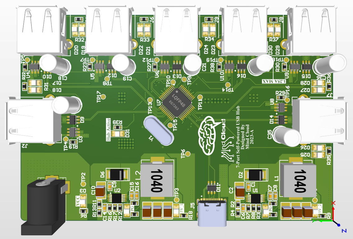
The main reason to do this is to provide the ground reference required for digital components clustered on the top layer, such as in the PCB example shown below. This board contains many digital circuits and power circuits, and both of these circuits benefit from the ground plane on L2. This project is a USB hub, so it includes multiple differential pairs which need ground to provide reasonably small trace widths. For the power circuits, nearby ground provides EMI suppression from switching regulators.
This USB hub uses SIG/GND as the outer layer pair to provide easy differential pair design for the USB lanes. Design submitted by Hany Hamza.
Bottom Half - PWR+SIG & GND
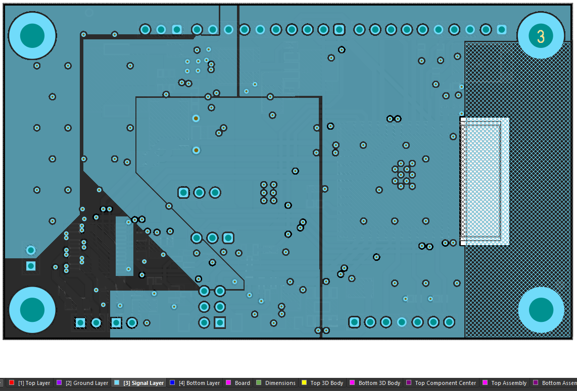
Assuming the top half is only being used for signal, the bottom half in the SIG/GND/PWR/GND stackup would only be used for power. The power layer can be divided up into multiple rails with different voltages, or it can be used as a complete plane at a single voltage. The former is a typical approach in some digital systems in order to support many isolated rails in some processors and ASICs.
This 4-layer PCB stackup defines L3 as a signal layer, but it is being used as a power layer with multiple rails. Design submitted by Kombo Chiganze.
If you don’t have multiple voltages, there is nothing wrong filling in with copper, it will be quite easy to reach power pins on components without needing to route traces in the component layer.
I like to bring up the point that it is okay to do this even if you are not operating at high current. Consider the calculation results from an IPC-2221 calculator or IPC-2152 calculator; the currents that large rails can handle could be quite high, but that doesn’t mean you cannot use large rails when currents are low.
Here is a summary of how to use copper regions for different power requirements.
|
High currents at a single voltage |
|
|
High currents, multiple voltages |
|
|
Low currents, single or multiple voltages |
|
In all of these instances, you could provide additional space in your power layer for signal traces. The ground layer on L4 will help shield these signals, which will make the design attractive for analog signals. Be careful with this as any noise in the power layer can couple into inner signals, so low-level analog signals might be in danger of receiving noise from noisy power rails.
Whether you need to build reliable power electronics or advanced digital systems, use the complete set of PCB design features and world-class CAD tools in Altium Designer®. To implement collaboration in today’s cross-disciplinary environment, innovative companies are using the Altium 365™ platform to easily share design data and put projects into manufacturing.
We have only scratched the surface of what’s possible with Altium Designer on Altium 365. Start your free trial of Altium Designer + Altium 365 today.

About Author
Related Resources
Table of Contents
Design to Release, Without the Friction
- Keep reviews tied to the right version
- Reduce handoff confusion and rework
- Spot sourcing and release risk earlier
- Work solo, share when needed
Get Started
Thank you, you are now subscribed to updates.

