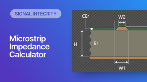
What Is Signal Integrity?
Many of the PCB layout and routing guidelines in use today, even for moderate speed signals and devices, are meant to ensure signal integrity. If you’re new to PCB design and you’ve never experienced signal integrity problems, the concept of ensuring signal integrity in a design might seem esoteric. Modern PCBs can experience many problems that can be solved or prevented with some simple layout practices. Signal integrity practices focus on identifying and fixing these problems in a PCB layout such that a digital or analog signal does not become distorted during propagation and can be recovered during its travels on an interconnect.
In this guide, we want to give a short overview of some signal integrity problems that can arise in a PCB layout, as well as some of the basic solutions to help solve these problems. By implementing some of these basic practices early in the design phase, it will be much easier to ensure signal integrity once the board is routed.
Basics of Signal Integrity
In the simplest sense, the goal of implementing signal integrity practices into PCB layout and routing is to ensure that a signal is not degraded as it transfers from a driver component to a receiver. In other words, we want to ensure the signal that appears at the end of an interconnect matches the signal that was injected at the beginning of the interconnect. While a signal will never truly experience no distortion, some basic practices can help minimize any potential signal distortion such that the receiver component always registers the correct signal.
There are some standard design practices that help ensure this, which begin during schematic capture and layer stack design. In fact, many signal integrity, power integrity, and EMI/EMC problems can be solved with appropriate stackup design and layer assignment for power, ground, and routing. Other simple solutions involve appropriate capacitor selection, impedance calculation, and understanding the limits of single-ended vs. differential traces.
Signal integrity is both an interconnect level problem, as well as a systems-level problem. Interconnects comprise pads, transmission lines, vias between PCB layers, and any components encountered along the way. At the systems level, there are driver and receiver components that generate and interpret the signal, respectively. Because there has been greater appreciation between the interaction between components and interconnects, EDA solutions providers have focused more on system-level simulation that looks at optimizing interconnects for specific high-speed protocols. This is very important as high-speed signaling protocols have become more advanced and run with faster edge rates.
When Should You Worry About Signal Integrity?
Technically, any design will have some signal integrity problems, but they generally do not interfere with the functionality of a product or create excessive noise until you are working with high speed digital signals or high frequency analog designs. In these cases, there are multiple problems to consider:
- Accurate impedance calculations to prevent signal reflections
- Losses and dispersion during propagation on long interconnects
- Crosstalk caused by fast switching digital signals
- Excessive radiation losses, which can appear as strong noise in EMC tests
- Overshoot and undershoot in digital signals due to excess inductance (ground bounce)
- Coupling of high frequency signals through parasitics
- Skew and resonant signal loss due to fiber weave
- Jitter, either due to random edge transition fluctuations, or due to SI/PI/EMI problems
- Additional losses due to copper roughness along the length of an interconnect
These are more difficult to address when operating at high frequencies, or at faster switching speeds used in high speed digital boards. However, to ensure a design does not fail due to these problems, there are some simple design steps that can be implemented to ensure signal integrity.
Start With Your Stackup
A major part of ensuring signal integrity is to clearly define ground and to keep ground near important traces during routing. A properly designed stackup, selection of power and ground planes, and designation of signal layers will help solve most EMI and signal integrity problems. There is also an important, beneficial effect on power integrity when stackups are designed properly.
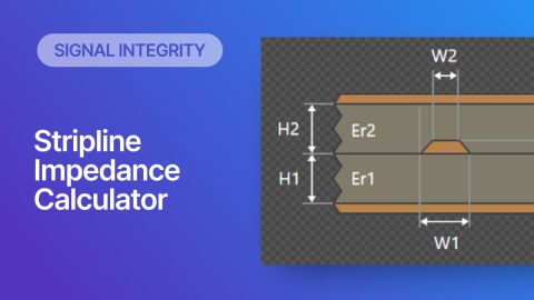
A typical arrangement involving alternating signal, power, and ground layers is shown in the stackup below. In this example, the design uses ground layers adjacent to signal layers to provide shielding, a low-impedance return path, and the ability to define controlled impedance lines (striplines or microstrips). Providing a low-impedance return path with well-defined trace impedance and ground near signals helps prevent reflections, reduces radiation and reception of EMI, and provides shielding from signals on different layers.

It is well-known that the layer thickness for microstrips, striplines, or coplanar arrangements will influence losses in digital or analog signals. Judiciously choosing the dielectric thickness in signals layers that need to support high speed/high frequency signals addresses one aspect of losses as mentioned above. In addition, selecting proper materials and plating materials for exposed traces can provide lower losses at high frequencies, such as in mmWave designs that require precise signal integrity. Taken together, these steps can help ensure signals experience low losses as they are routed to the end of an interconnect.
- Learn more about designing traces for impedance controlled routing
- Learn more about high frequency materials for advanced RF PCBs
The Importance of Impedance and Routing
Once the stackup is determined and important components have been placed, the layout is completed by routing traces. Signaling standards used in digital interfaces and high frequency analog signals will specify impedance requirements that should be obeyed to ensure signal integrity and prevent problems in high speed channels. During routing, careful attention needs to be paid to some important geometric qualities of traces on the PCB:
- Single-ended and differential impedance
- Consistent spacing and length matching tolerances for differential pairs
- Ensuring a tight return path throughout a route with grounded vias and uniform planes
- Minimizing via transitions and excessive bends at high frequencies (10’s of GHz)
- Removing via stubs on the highest speed/frequency routes
The first two points are designed to ensure that the impedance along a route does not deviate from the design value specified in the relevant signaling standard. The third point addresses EMI and noise coupling by ensuring the return current generated by high-speed/high-frequency signals has low inductance. The final two points address the need to eliminate loss and reflection at any impedance discontinuity along a route. Elements like connectors and vias may have input impedance that deviates from the required impedance value, thus design rules are used to help ensure these targets are met in the design.

Routing tools in your PCB design software can take your routing requirements and encode them as design rules to help ensure you meet your impedance, spacing, via count, and return path goals. Applying backdrilling represents a cost tradeoff against signal integrity, so it should only be applied on the fastest digital signals, and only if some alternative routing scheme cannot be implemented to eliminate the need for backdrilling. In total, these measures can address problems that arise from reflections, such as intersymbol interference in an eye diagram and standing waves on mismatched transmission lines.
Identifying Signal Integrity Problems
Signal integrity problems need to be identified in simulations or measurements. Ideally, simulations should be performed during the design process to help identify any signal integrity problems before creating prototypes. One common practice is to create test boards for a design so that measurements can be taken before a design is put into high volume production. No matter how you plan to identify signal integrity problems, these tasks should be completed before scaling a design into high volume production.
Simulations During Routing
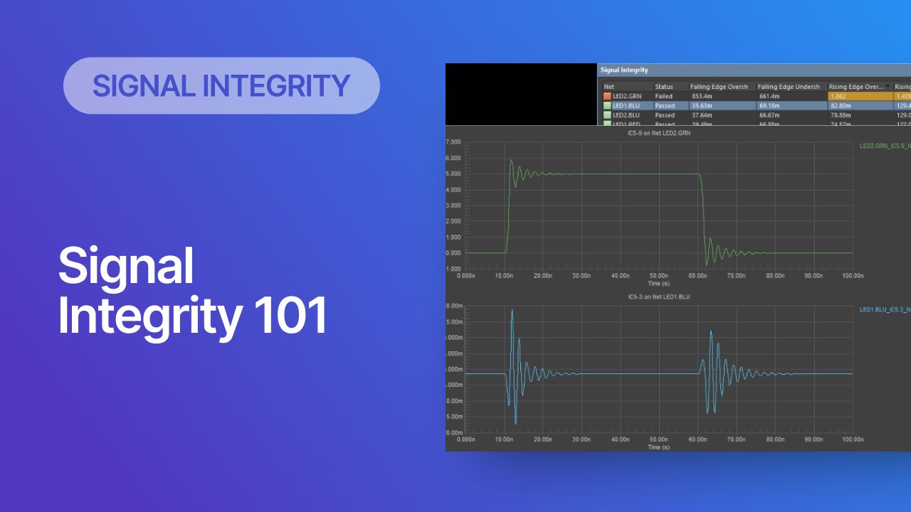
During the design phase, some of the more advanced ECAD packages can be used to identify signal integrity problems in some simple simulations. Two standard simulations that can be performed together are crosstalk waveform calculations and ringing/reflection waveforms. Both simulations require defining the logic family for the driving component in the PCB layout, which can be found in datasheets. These simulations give a very clear view of the effectiveness of terminations and spacing between interconnects, which can be seen in an interconnect’s transient response (see below).

Other points to check during routing include:
- Overshoot and undershoot
- Rise time/fall time during switching
- Skew in parallel buses and differential pairs
- Return path continuity
These points can be checked with your online simulation tools in advanced ECAD packages for PCB design. Once the design is routed, an in-application simulation tool can calculate these points to ensure signals on each interconnect sit within noise margins and have the required response as viewed at the receiving component. By identifying these problems early in the design process, many signal integrity problems can be solved early, ideally eliminating complex and time-consuming redesigns.
Signal Integrity Testing
Although there are several tests that can be performed to evaluate signal integrity, two of the most important for digital designs are S-parameter measurements with a vector network analyzer (VNA), and eye diagram tests with a standard test bitstream. The time-domain counterpart to an S-parameter measurement is a time-domain reflectometry measurement, which requires a special instrument to supply a pulse to an interconnect or device under test. Although eye diagrams and bit error rate calculations are normally performed with an oscilloscope, some VNAs can generate eye diagrams.

Eye diagram measurements and extracted bit error rates are critical for evaluating digital channels. They provide a summative measurement that allows quantification of jitter, ISI due to signal reflections, losses, and the need for compensation through equalization. Some simple changes to a design can be identified from these measurements, and the extracted signal integrity metrics can be compared with other simulations or calculations.
S-parameters, as well as other network parameter simulations or measurements, live in the frequency domain. They allow a design to be qualified in terms of its maximum possible data rate, transmission frequency, losses, or reflections due to impedance mismatches. For long interconnects, the more important quantity is S21 or insertion loss as these channels are dominated by dielectric, copper, and radiation losses. In short channels, the more important quantity is S11 or return loss as there is the potential for strong reflections and resonance in short to moderate length channels.
More Complex Simulations for SI, PI, and EMI/EMC
Once a layout is completed and is ready for signoff, the design should first be put through a more advanced simulation tool that can look at the entire system, rather than looking just at the individual interconnects. These simulation packages take data from the finished PCB layout and calculate the electromagnetic field directly from Maxwell’s equations. Standard mechanical file formats (IDX) and specialty simulation data file formats can be used to import design data into external simulation programs, allowing EMI/EMC, PI, and system-level SI problems to be identified before prototyping and production.
- Learn more about using simulations to identify near-field EMI
- Learn more about sharing your simulation data through the cloud
PCB routing is much easier when you use the complete set of PCB layout tools in Altium Designer, available within Altium Develop. The integrated design rules engine in Altium Designer automatically checks your routing as you place traces, allowing you to spot and eliminate errors before you finish the board. Every Altium Develop user also has access to a dedicated workspace, where projects, component data, manufacturing data, and any other project documentation can be stored and shared with collaborators.
Whether you need to build reliable power electronics or advanced digital systems, Altium Develop unites every discipline into one collaborative force. Free from silos. Free from limits. It’s where engineers, designers, and innovators work as one to create without constraints. Experience Altium Develop today!


