










The Best Flash Memory Storage Solutions: Is NOR or NAND Ideal for Your Project?


The two major types of flash memory are NOR Flash and NAND Flash. Learn about the differences between these types of flash and how they impact your embedded system in this article.
When designers are looking for long-term storage in their electronic products, they typically look to two different options: an EEPROM or flash memory. An EEPROM is a simpler erasable device that is often used with small microcontrollers where large amounts of data do not need to be stored or recalled repeatedly. They are a versatile long-term solution for memory in many devices, and they still enjoy widespread use today.
On the other hand, devices that need to store or recall larger amounts of data or that run on a larger embedded application will predominantly use flash memory. Typically, large firmware binaries are written to a flash chip rather than directly to a microcontroller or ASIC, as the internal memory in these processors is limited.
There are two types of flash memory: NAND flash and NOR flash. Let's look at the differences between these types of memories in this article.
How Flash Memory Works
Flash memory is a non-volatile storage technology that retains data after power is removed by trapping electrical charge in floating-gate transistors. Each cell stores one or more bits depending on the architecture, and data is organized into pages and blocks that can be erased and reprogrammed electrically without removing the device from the circuit. This erase-before-write constraint is fundamental to how all flash memory operates, and it shapes the performance characteristics that differentiate NOR and NAND architectures at the system level.
NOR and NAND flash differ in how their cell arrays are wired. NOR flash connects cells in parallel, which allows the host processor to address and read any individual byte directly, making it suitable for execute-in-place firmware storage. NAND flash connects cells in series, which reduces die area and cost per bit but requires data to be read in pages and written through a controller with wear-leveling and error correction logic. These architectural differences produce distinct performance, capacity, and endurance tradeoffs that drive the selection decision in embedded system design.
NOR Flash | NAND Flash | |
Read access | Random byte-addressable, fast | Page-based, slower random access |
Write speed | Slow | Fast |
Erase speed | Slow (sector erase) | Fast (block erase) |
Capacity range | Low to moderate (KB to hundreds of MB) | Moderate to very high (MB to TB) |
Cost per bit | Higher | Lower |
Endurance | 10,000 to 100,000 erase cycles | 1,000 to 100,000 cycles depending on cell type |
Execute-in-place | Supported | Not supported |
Error correction required | Minimal | Yes, mandatory |
Typical use | Bootloader, firmware code storage | Mass storage, data logging, file systems |
Flash Memory Packages
Flash memory is most commonly available as ICs in SOIC, WSON, or TSOP/TSSOP packages. For high memory capacity, BGA packages are available with coarse ball pitch (1.0 mm) and low pin count. The BGA versions of these components will typically have standard fan-out with just a few power and ground balls, and the rest of the balls being configuration and data pins.
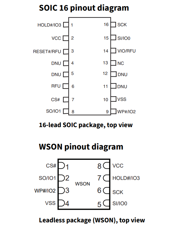
For the SOIC, WSON, or TSOP versions of these components, the pinout is often standardized so that flash chips with different capacities can be used as drop-in replacements for each other. For example, the typical SOIC-16 package pinout for a NOR flash chip is shown in the image below. The configuration pin functions are standardized, as are the required voltage values on the power and IO pins. Although these components may have lower memory capacity per unit area, this gives much more flexibility to swap chips with different capacities as needed.
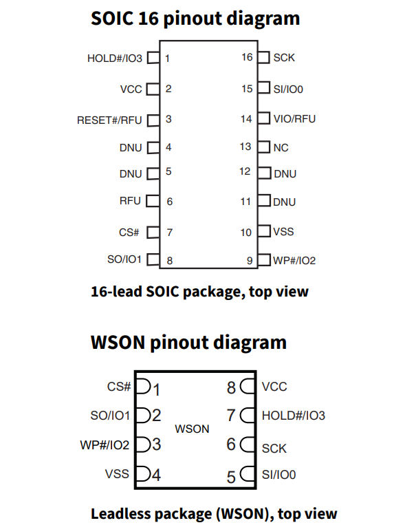
The majority of flash memories use an SPI bus to read and write data. The clock frequency for accessing data will be given in the basic description of the flash chip, and the firmware running on the system host will need to set the appropriate clock frequency to accommodate. This can be seen in the pinout above.
On a typical flash chip, a subset of pins are required for basic operation and others enable optional features:aaaa=
Mandatory pins: VCC (power supply), GND (ground), SCK (SPI clock), SI/MOSI (serial data input), SO/MISO (serial data output), and CS (chip select, active low) are all required to bring the device up and communicate over SPI.
Optional and configuration pins: WP (write protect, active low) enables hardware write protection on one or more protected regions of the array; leaving it pulled high disables the feature. HOLD (active low) suspends an active SPI transfer without deasserting CS, which is useful in multitasking firmware contexts. RESET (active low) forces the device to a known idle state and is good practice to wire up even if firmware does not actively use it.
Flash Memory Chips on a PCB
As these chips have an SPI interface, they are operating at the low end of what we would consider to be high-speed. Therefore, most designs will use four layers to provide a solid ground reference for the SPI interface. As these devices use SPI or QSPI, there is no impedance specification, and termination is typically not used since flash chips tend to be placed close to the system host processor. A basic entry-level stackup looks like the four-layer sig/gnd/gnd/sig design shown below.

Because we review a large number of user-submitted PCB designs, we often notice that designers will use sig/gnd/pwr/sig as the stackup. As more high-speed interfaces are added to a board, this stackup becomes less desirable, and it would be preferable to have two ground planes to support high-speed routing on both outer layers. To learn more about the four-layer stackup with a power plane, read the resources below:
A typical flash chip option suitable for most circuit boards is the component shown below from Macronix. These flash memory chips have been used in several designs, including in our Ethernet switch project, which you can learn more about in this linked article. A memory capacity of 128 Mbit or 256 Mbit is a typical high-end value for flash chips in SOIC or WSON packages.
Once you get to higher memory capacities, such as 512 Mbit or higher, the package option will typically switch to a BGA. However, these BGAs do not have high pin count, and only two signal layers should be needed to fully fan out the device.
To power these devices, a decoupling capacitor is recommended at the power pin connecting to the ground plane, particularly when using routed power in a sig/gnd/gnd/sig circuit board. When a power plane is present, there is more freedom to place the decoupling capacitor, particularly on the BGA versions of these components. To learn more about decoupling capacitor placement for these devices, read this linked article.
More Memory Beyond Flash
Once the long-term storage requirement reaches multiple Gbit, designers usually move beyond discrete serial flash. The two standard options are a PCB-mounted eMMC device or an SD card installed in a board-mounted connector. eMMC is a specific type of flash storage package that includes both memory and a built-in controller; it provides fixed storage soldered directly on a PCB, while an SD card provides removable storage that can be replaced or upgraded.
SD cards use NAND flash, but the card can hold much more memory than a typical PCB-mounted flash IC. The larger package can contain several stacked NAND dies, and high-density TLC or QLC cells further increase capacity. The card also includes a controller for error correction, wear leveling, bad-block management, and address translation. This allows the host to access a large storage volume without directly managing the NAND array.
An eMMC device combines NAND flash and a storage controller in one BGA package. The controller handles error correction, wear leveling, bad blocks, and logical address translation, which reduces firmware and processor requirements. For PCB design, the main concerns are package fanout, supported I/O voltage, bus routing, decoupling, and processor support for the required eMMC mode.

Typical eMMC specifications relevant to PCB designers include:
- BGA packaging with a defined ball map and fanout requirement
- One-bit, four-bit, or eight-bit parallel data bus
- Separate clock, command, and data signals
- 1.8 V or 3.3 V signal levels
- Separate core and I/O power rails with local decoupling
eMMC is usually the lower-risk choice for fixed high-capacity storage because the controller and flash-management functions are integrated. It simplifies software development and reduces validation work, but the BGA package is difficult to replace and provides limited control over wear management. Therefore, if you want your product to avoid some obsolescence issues or allow the user to upgrade their storage capacity, an SD card is the better option.
Whether you need to build reliable power electronics or advanced digital systems, use Altium’s complete set of PCB design features and world-class CAD tools. Altium provides the world’s premier electronic product development platform, complete with the industry’s best PCB design tools and cross-disciplinary collaboration features for advanced design teams. Contact an expert at Altium today!

About Author
Related Resources
Related Technical Documentation
Table of Contents
Solutions for Every Role and Team
- Discover and evaluate design options earlier
- Develop in one shared workspace
- Scale with control and compliance
- Connect every stage of hardware development
Learn More
Thank you, you are now subscribed to updates.



