


The Hateful Five of PCB Manufacturing


You just completed your last design review, got that needed approval signature, and the finish line has never been closer, or so you think. Even after your components are sourced and your board is laid out perfectly, the biggest challenge is yet to come - ensuring that all those months of design and team effort don’t go to waste when it comes time to communicate design intent to manufacturing.
But how do you navigate this stage of your post-design process? You’ve got all the tools you need to output all the files your manufacturer will want. But we all know the translation process from digital bits to physical goods is never that simple and straightforward. The truth is, you can put months of hard work into designing the perfect board layout, only to completely drop the ball by not communicating design intent clearly in your manufacturing documentation.
If there’s one single source of truth to hold your documentation process to, it’s defying conventional wisdom with more details being better, not less. So what are some of the fine details that most PCB designers commonly overlook in their documentation process? We’ve outlined PCB manufacturer’s Hateful Five to be aware of in your own documentation process, so you’ll never get your design rejected again.
#1 - Incomplete PCB Documentation Content
It might seem like a no-brainer, but the path from transitioning your PCB design process and specifications to all the essential files your manufacturer needs is never a straightforward path. And all it takes to throw a wrench into your entire production process is to have one missing piece of documentation that sends your manufacturer into a frenzy. Here are some guidelines to keep in mind to avoid having incomplete PCB documentation content passed off to your manufacturer:
-
If you’re using a PCB design tool that requires you to manually generate output documentation, pay close attention to the files you are outputting and keep them organized in a single repository.
-
Confirm with your manufacturer exactly what manufacturing files they require and in what format (Gerber, ODB++, etc…) before sending them anything.
-
Never send your manufacturer a single, internal CAD file and assume they have the software to read it..
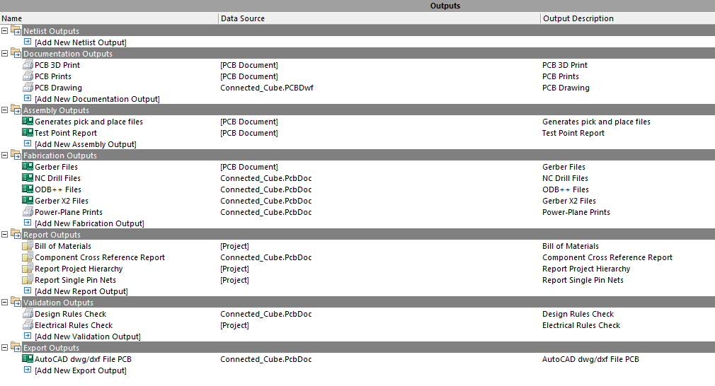
To put it simply - a complete PCB documentation package should contain all the files required by your manufacturer, all organized in a file format and structure that is easily interpreted without any guesswork. Any redundant or errant files found by your manufacturer will only add delays to your manufacturing process, and that’s the last thing you want to deal with.
Complete Documentation Data Package (Output Job Files)
#2 - Not Indicating Your Class Type
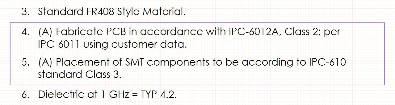
While Class 2 is the industry default for PCB documentation, your master drawing will change drastically if you happen to design with a different Class (1 or 3). Because of this, it’s important to clarify exactly what Class is being used with the following guidelines:
-
In order for your manufacturer not to assume a standard Class 2 process is required, it’s recommended to call out the preferred build standard of whichever Class you need on both your PCB fabrication and assembly drawings.
-
In the event that you have varied process preferences for specific components, you’ll need to indicate that they require different treatment than what your assembly drawing specifies. (e.g. having a Class 2 assembly with a Class 3 hole fill requirement).
Indicating the Class requirement in your drawing package will ensure that your PCB gets processed properly, while also assisting during the technical review process. This critical piece of information will ultimately allow your manufacturer to provide the most accurate quote possible while also successfully manufacturing your board.
Class Type PCB Drawing Note
#3 - Missing Solder Specs
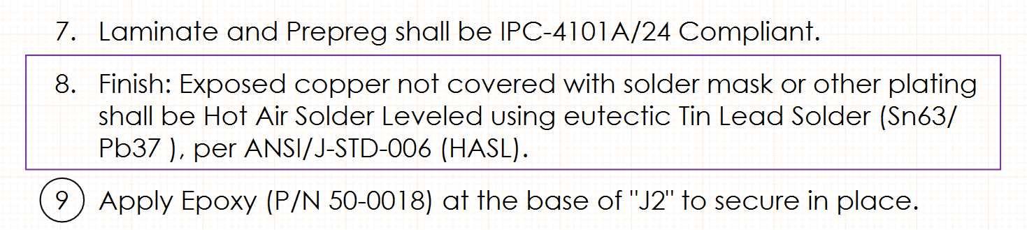
In years past, many manufacturers weren’t overly concerned about whether a PCB needed to be lead-free or not. But times have changed since 2004, and with the introduction of RoHS (Restriction of Hazardous Substances) PCB manufacturers are required to support a variety of solder and flux combinations. Here are some guidelines to follow to properly document your design for RoHS requirements:
-
Any business that sells applicable electronic products to RoHS countries must comply with this directive and indicate compliance in documentation notes.
-
While RoHS might be a standard rather than an exception now, it’s important to indicate where RoHS specifications are not needed on your documentation packages with a non-RoHS designator.
Whether we like it or not, RoHS compliance is here to stay. To stay ahead of the game, always ensure that you’re properly documenting your PCB with RoHS or non-RoHS specific designators as needed to avoid having your board production delayed.
Assembly/Bare Board Finish PCB Drawing Note
#4 - Missing ITAR Requirements
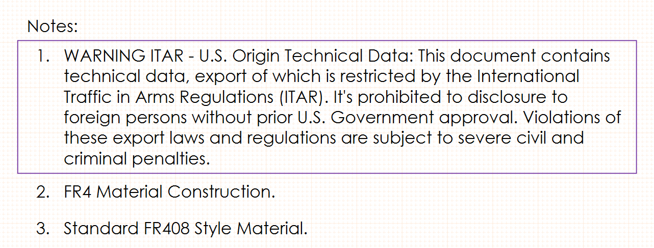
A quick fact to put #4 in perspective - one IPC study found that as much as one-third of PCBs produced for the defense industry are produced abroad. To put it simply, the financial and legal issues associated with having your design sent overseas and handled by a non-US person is something that needs to be taken seriously and documented thoroughly. Here are some guidelines to keep in mind for documenting your ITAR (International Traffic in Arms Regulations) requirements:
-
As more aspects of the PCB design industry supply chain become outsourced, engineers must specify ITAR requirements in their documentation to ensure their data packages are handled properly.
-
Ensure that you are documenting your ITAR requirements in the correct location. Some manufacturers receive ITAR specs on Purchase Orders instead of the fabrication and assembly drawings.
By carefully documenting your ITAR requirements, you’ll avoid putting both yourself and your manufacturer at risk for accidentally mishandling sensitive ITAR data. And that’s the last issue you’d ever want to talk to your boss about.
ITAR Compliance PCB Drawing Note
#5 - Missing Layer Sequences
Last but not least, missing layer sequences. The specific arrangement of your layer stackup is a critical component of your electronics design, especially for high-speed digital designs requiring matched impedance transmission lines. Here are some guidelines to be aware of when documenting layer sequences:
-
You can indicate the layer numbers in the copper image and place the logical number in each layer (starting from the top, 1 for the top layer, 2 for inner 1, 3 for inner 2, and so forth). If this indication method is used, remember to position the numbers in a way where they won’t overlap.
-
Include in your assembly and fabrication drawing a clear stackup drawing that includes all copper layers, soldermask, overlay layers, and any additional layers in the correct sequence and also with the corresponding correct data file names.
-
Name each layer file in a manner that clearly shows the correct sequence (e.g. Top, Mid1, Mid2,.., Bottom).
When a designer forgets to include their layer sequences in their documentation the result is never fun with improperly functioning boards and resins. With the guidelines above you should be able to clearly communicate design intent to manufacturing so you never run into this problem.
Ideal PCB Drawing Layer Stackup Legend W/ Gerber Files Names
Rounding Up the Results
There you have it - the Hateful Five that every PCB manufacturer dreads to get in a designer’s documentation package. This was just a small list of every possible guideline or specification that you’ll need to have included in your documentation. But by including the above in your personal set of best practices, you’ll be well on your way towards minimizing any production delays due to errors, miscommunications, or missing files. Take a look at Draftsman® to help you out with some of these documentation Woes.
Got your own set of do’s or don'ts for manufacturing? Share your thoughts in the comments below!
Check out Altium Designer® in action...
Powerful PCB Design
About Author
Related Resources
Table of Contents
Design to Release, Without the Friction
- Keep reviews tied to the right version
- Reduce handoff confusion and rework
- Spot sourcing and release risk earlier
- Work solo, share when needed
Get Started
Thank you, you are now subscribed to updates.


