What is a Power Sequencer IC?

At a Glance
Power sequencer ICs and power switch ICs can be implemented in a programmable mixed-signal IC approach that simplifies system design.


Power sequencer ICs are an essential component in many electronic systems that use groups of power regulators for different subsystems and circuits. Simple power sequencing strategies can be implemented with a dedicated power sequencer integrated circuit, a microcontroller, a small FPGA, or a set of analog components. Another solution that consolidates these options into a single component is a mixed-signal IC, which can be programmed to perform power sequencing and monitoring.
Look at each of these approaches in detail in this article. These range from very simplistic, such as delayed power-up of regulators, to more advanced, where monitoring of one power regulator is required before turning on another power regulator.
System Topologies That Use Power Sequencer ICs
Many products use groups of power regulators that can be toggled on or off in a specific order or based on application logic. Voltages are often grouped based on function or based on which parts of the subsystem they are powering. Because power regulators may need to be turned on in a specific order and based on certain system conditions, power sequencer ICs are often used to perform tasks.
Power sequencer ICs fall into a few different categories depending on how they toggle power regulators:
- Power sequencers that toggle regulators on and off based on delay
- Power sequencers that toggle based on reading a PGOOD (or PG) pin
- Power sequencers that actively measure and monitor system power
The first two of these solutions are totally passive, and they can be implemented as integrated components or as a set of analog circuits. The final option requires some programming to implement, but it becomes a standard requirement in more complex systems with multiple regulator stages and voltages. Contemporary examples include RF systems, space systems, precision measurement systems for scientific or industrial settings, robotics, and UAS.
Basic Power Sequencer ICs With Delay-Based Sequencing
The simplest power sequencer ICs implement delay-based sequencing, where the sequencer toggles power regulators in a specific sequence with a fixed delay. These devices have very simple circuitry and typically only require a few capacitors to stabilize the I/Os pins and power pin. These components could more accurately be called power switch ICs as they provide simple toggling of power stages without sensing or managing power delivery.
A functional example is shown in the block diagram below.
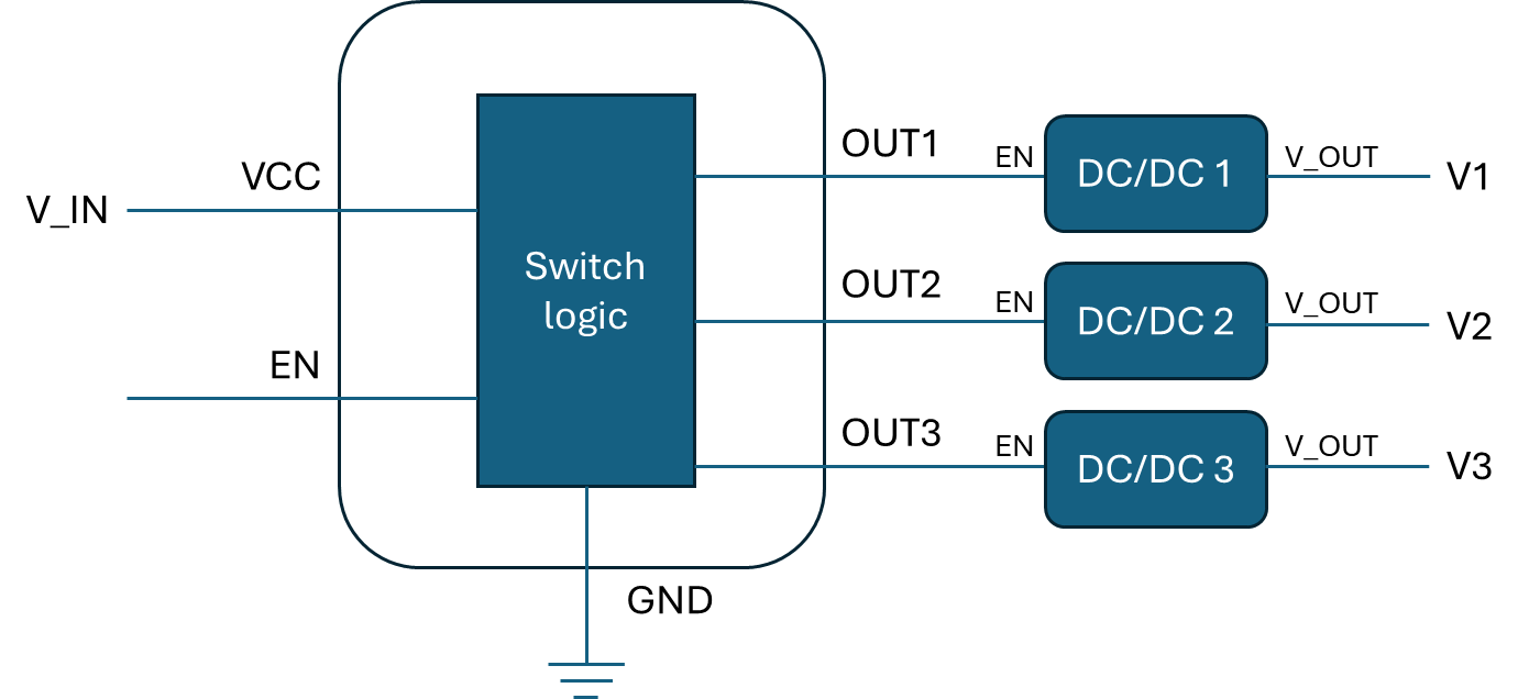
Simple power switch IC application for power sequencing.
The EN pin can be toggled with a microcontroller GPIO pin or it could be tied to the VCC pin with a resistor. The outputs then toggle the EN pins on DC/DC converters, which may use a variety of input voltages which are not equal to V_IN.
For basic load switching functions, this type of component is an excellent choice. For more complex systems which are sensitive to turn-on rate and transients, there are several disadvantages of this type of component:
- Power-up and power-down times and delays are not always configurable
- There is no monitoring of the output voltages from the regulators (V1-V3)
- There is no direct feedback mechanism for fault reporting
- There is no way for the switch IC to monitor that the output voltages have settled to their target values
If a systems designer wanted to implement these additional functions, additional custom analog circuitry and/or ADCs would be required. However, there are some methods and components with additional monitoring through PGOOD pins, which can be used to cascade each regulator in the power stage.
Basic Power Sequencer ICs With PGOOD Sensing
A more advanced type of power sequencer IC will also toggle the EN pins of the system power regulators in a specific sequence, similar to the power switches mentioned earlier. However, these can sense the PGOOD pins of each power regulator (if these are present) and use these as the trigger to toggle the next regulator in the series.
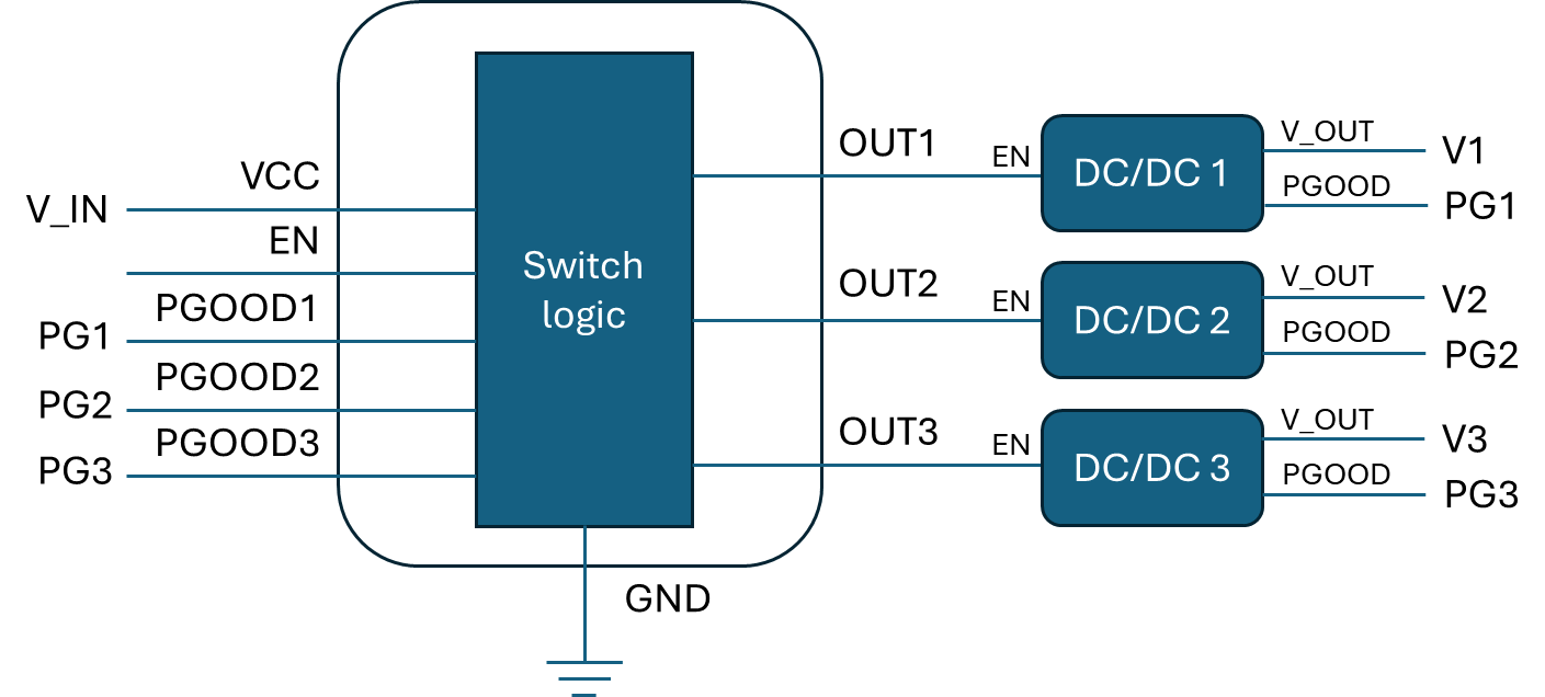
Normally, this could be implemented by using the output of one regulator (V1 for example) as the gate voltage on a MOSFET to toggle the EN pin of the next regulator, but this increases the total component count. This system can suffer from some of the same drawbacks as the power switch IC approach unless regulation and settling are monitored in each DC/DC converter stage.
As systems get more complex, more detailed monitoring and logic are needed to implement power sequencing. This is where system firmware/software will take a more central role in the power sequencing process.
Microcontroller/FPGA-Based Power Sequencing
If an external enable toggle is used on the EN pin of a power sequencer IC, then this could be implemented using a single pin on an MCU or FPGA. This would effectively move the power switch IC functions into the MCU/FPGA via an I/O pin. An example is shown below.
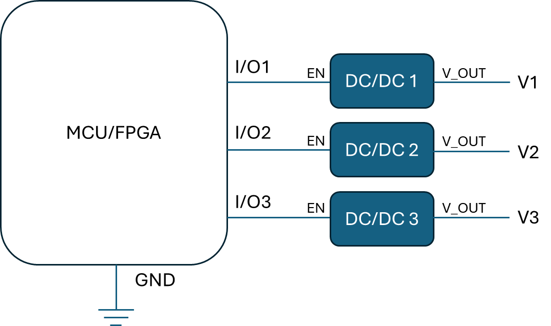
If level shifting is needed to toggle the enable pin, which may be the case when an MCU/FPGA I/O has lower logic level and is used to toggle a buck converter, an N-channel MOSFET and resistor divider may be used as a buffer switch.
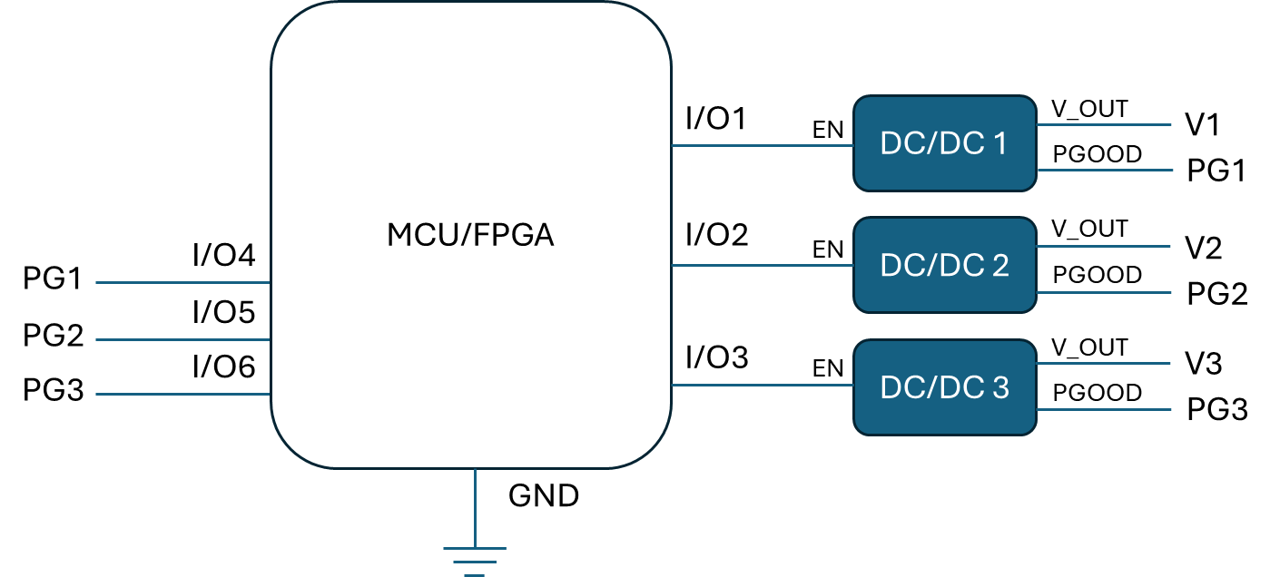
If the power regulators output a PGOOD signal that needs to be monitored, these outputs can be monitored with the processor’s I/O pins and the next regulator can be toggled on based on logic in the embedded application.
Things get more complex and require more components when real-time monitoring of the output power is required. The power sequencing sub-system may need to monitor output voltage transients and settling, output current, and noise levels, and it may implement startup/shutdown/fault logic based on these measurements.
For example, sensing voltage and current outputs from regulators and using these for sequencing could require multiple ADCs, or at least a multichannel ADC. However, multiple ADCs will most likely be required with a demand for different references, input filtering/amplification, and available input range for each regulator. For current sensing in moderate power systems, a current sense amplifier is the safest and most accurate choice rather than reading across a current sense resistor.
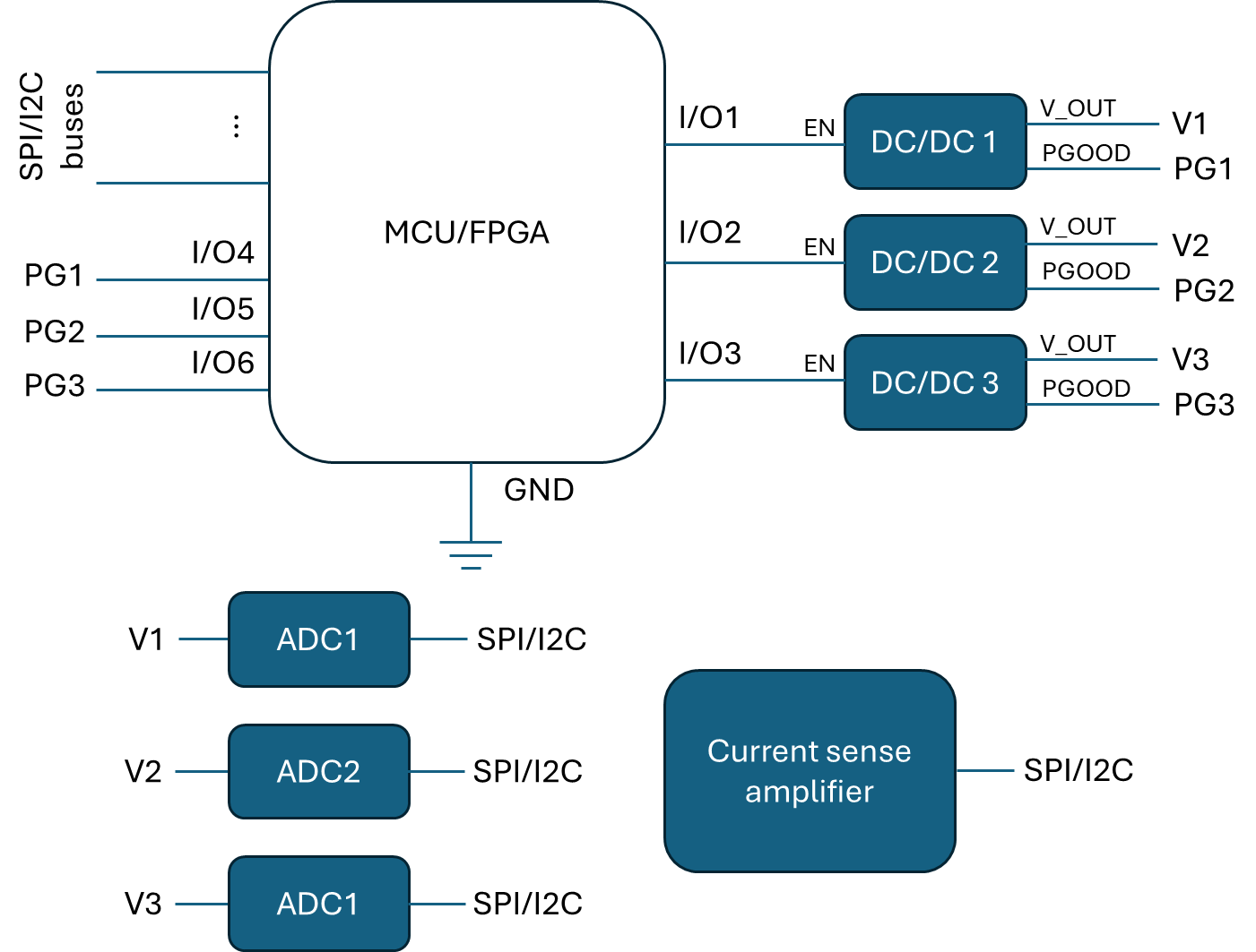
Simple groups of power regulator circuits (small LDOs, small bucks/boosts) could likely use only the ADC pins on the MCU, and the real-time sensing is implemented in application firmware. However, more complex high power systems will need these additional components.
Mixed-Signal IC-Based Power Sequencing
A more compact solution that implements the can be used to implement digital logic and analog processing is a programmable mixed-signal IC. These devices can be configured (and reconfigured) to perform specialized analog measurements in a programmable matrix, similar to what is implemented in an FPGA for digital logic.
This programmability of the analog processing matrix greatly simplifies implementation of many sensing and control tasks such as one would use in power sequencing tasks. It does this by consolidating most of the analog processing tasks into a single package rather than requiring a group of external analog components and circuits. This potentially reduces the entire power sequencing subsystem into two components: the system host (MCU or FPGA) and the mixed-signal IC. An example implementation is shown below.
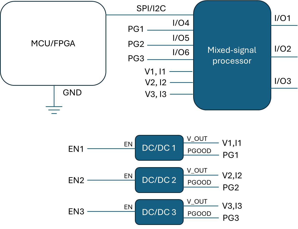
If additional GPIOs are available on the mixed-signal IC or the MCU/FPGA, those GPIOs could be used for example in triggering system resets, providing fault indicators, or toggling other system peripherals which might be sensitive to power supply fluctuations.
Standalone Programmable Mixed-Signal IC
A final approach is to use the programmable mixed-signal IC as a standalone component, especially considering the fact that not all power systems include microcontrollers for monitoring. This essentially implements the above block diagram, but with the serial interface on the mixed-signal IC broken out to a connector for programming purposes. These processors can implement their own digital logic and internal analog processing, so an MCU or FPGA is not required for power sequencing.
Today, the only programmable mixed-signal matrix products that can perform these functions is the GreenPAK product line from Renesas. GreenPAK is a set of hardware components and associated software solutions that help systems designers quickly implement mixed-signal applications like power sequencing and monitoring. Renesas provides a Solution Cookbook and documented code examples for a simple power sequencing application, as well as many others.
Whether you need to build reliable power electronics or advanced digital systems, use the complete set of PCB design features and world-class CAD tools offered by Altium to implement your GreenPAK solutions. Altium provides the world’s premier electronic product development platform, complete with the industry’s best PCB design tools and cross-disciplinary collaboration features for advanced design teams. Contact an expert at Altium today!
Related Resources

Related Technical Documentation

Thank you, you are now subscribed to updates.

