






Why Do PCB Designers Use IPC Standards?

At a Glance
IPC standards exist to set expectations between PCB designers, PCB manufacturers, and PCB design software vendors.


Recently, I was reminded of the importance of industry standards for everybody involved in PCB design and production. All industry standards are hefty documents containing tons of information, and no individual has the capacity to memorize, nor will they ever use, every single standard in our industry. But the standards we have play an incredibly important role in setting expectations for anyone involved in design and manufacturing.
That setting of expectations might sound like it constrains designers, but it actually provides assurances that the boards they design can be produced, even in mass quantities. I'll give some examples of why this is so important and how to understand the evolution of electronics industry standards over time.
How to Understand Guidance in IPC Standards
I think the importance of IPC standards can be best illustrated through an example.
This conversation about IPC standards recently came up because I received a message on LinkedIn. The message was regarding the IPC-7351 standard, specifically the courtyard guidance found in Revision B and Revision C. Images showing the courtyard guidance for a leaded quad pack are shown in the two images below.
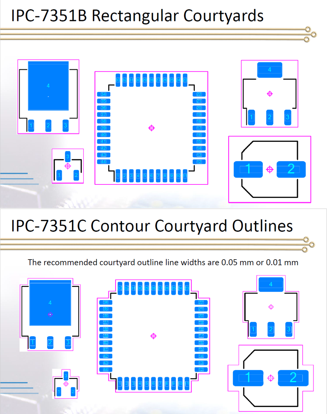
The question relating to these two images is simple:
- Which of these courtyard designs should be followed in a PCB footprint?
- Although the question seems very simple, the answer can be both simple and complex simultaneously!
First things first: the answer to this specific question is that either courtyard format can be used. Courtyards are used to standardize a placement boundary in a PCB layout and to standardize the distance between copper land pads for SMD components. These values are defined for low-, medium-, and high-density placement. If you understand the reasons for a courtyard layer in a component footprint, you will quickly understand the intention behind the IPC-7351C revision: it standardizes a new courtyard format to accommodate higher-density placement.
This creates two sets of expectations:
- PCB designers should reasonably expect that anyone creating footprints as a service, or providing free downloads for footprints as a service, will include this standardized boundary in a courtyard layer.
- PCB assemblers should expect that designers will place components right up to the edge of the courtyard limits defined in the IPC-7351 standard, and their assembly capabilities should be expected to accommodate this.
Ideally, both the footprint creators and the PCB assemblers will accommodate the allowances in IPC-7351C in this example. In this specific case, the guidance in the Revision C standard was created because designers were already doing this in higher-density designs, and PCB assemblers were, by and large, able to accommodate such placement in SMT processing. Therefore, the standard was updated to formalize these expectations between all parties involved in PCB design and manufacturing.
Other Examples Where IPC Standards Set Expectations
There are many other examples we can find where standards set expectations for design practices, reliability, verification, and safety. I've compiled a few of the more important examples below.
- Design practices: A great example from high-voltage design is IPC-2221B and IPC-2221C. These standards provide clearance values between conductors and give designers some assurance that a product will be reasonably protected from arcing.
- Material substitutions: IPC slash sheets, as defined in IPC-4101, define substitute material compatibility in terms of handling and processing.
- Test methods: Testing standards have been developed to ensure that manufacturers are qualifying bare PCBs, PCBAs, and their processes using the same set of tests.
- Reliability classification: IPC product classes are related to the reliability of PCBs and PCBAs. This, in turn, defines certain design and manufacturing standards, such as via pad sizes for minimum annular rings and via plating thickness requirements.
There are other industry standards beyond the IPC standards that also perform the same function of setting expectations. For example, Ethernet standards dictate that any suitable Ethernet transformer should provide 2.1 kV galvanic isolation at peak voltage. Another great example is JEDEC-standardized packages, which define integrated circuit package sizes and lead formats. These packaging standards for integrated circuits ensure that, for example, all SOIC-8 packages are interchangeable with each other from a mechanical perspective.
Are PCB Designers Required to Follow IPC Standards?
The answer here is a bit complex. Designers who follow IPC standards tend to have a much higher chance of receiving PCBAs that are reliable, manufacturable at scale, and can be independently verified as such; this is a clear incentive to follow IPC standards wherever possible or applicable.
However, there are many instances where designers violate IPC standards for a variety of reasons, and this will not automatically mean that a product is not reliable or producible. Sometimes, the design practices implemented in a PCB will go above and beyond the IPC-standardized requirements because this is what a company may have found to be required to ensure the reliability and manufacturability of its specific products. Deviations from an IPC standard are certainly justifiable, and this doesn't mean that a product will receive a no-bid because of them.
That being said, if you do violate or ignore certain IPC standards, don't be surprised if a manufacturer says they cannot guarantee reliability or manufacturability at scale in certain areas. The CAM department at a manufacturer will do an extensive review of the PCB manufacturing outputs before approving a design for production, precisely so that they can identify these issues and inform the designer. This way, they cannot be held liable for a product that they believe will be at risk of failure.
Whether you need to build reliable power electronics or advanced digital systems, use Altium’s complete set of PCB design features and world-class CAD tools. Altium provides the world’s premier electronic product development platform, complete with the industry’s best PCB design tools and cross-disciplinary collaboration features for advanced design teams. Contact an expert at Altium today!

About Author
Related Resources
Table of Contents
Solutions for Every Role and Team
- Discover and evaluate design options earlier
- Develop in one shared workspace
- Scale with control and compliance
- Connect every stage of hardware development
Learn More
Thank you, you are now subscribed to updates.