Creating Multiple-Part Symbols for a PCB in Altium Designer


When you are designing electronic circuitry for printed circuit boards, creating symbols in your CAD system is part of the job. For the most part, you will be pulling symbols from different libraries, but every now and then you are going to have to build one yourself. Creating symbols in Altium Designer® is a straightforward operation - you can build a symbol manually or use an advanced symbol generator to do the heavy lifting of symbol creation for you.
But what about creating components that have multiple symbols in them? They are called gates or slots in the industry, and in Altium Designer they are labelled multi-part components. If you haven’t had to build one of these before, don’t worry. That’s exactly what we are going to talk about here--how to create a multi-part component. It’s a little more complicated than building a single symbol component, but you will end up with a good understanding of the process by the end of the article.
Why Use a Multiple Part Component in the First Place?
Altium Designer uses symbols to represent electrical components on the schematic. These components are made up of symbols with component information added to them, such as which footprint to use. This information is what makes a symbol become a component in Altium Designer. To create a symbol manually, you will draw the shape of the symbol and add pin information to it. Altium Designer also has a symbol generator which will do some of this work for you.
Multi-part symbols are the same as other symbols in Altium Designer; the only difference is that they have more than one symbol within a component. If you haven’t used them before, multi-part components are a very useful resource to use when creating a schematic. For instance, you can use a multi-part component to define a resistor pack, a connector, or a gated device. This is to place specific resistors, connector pins, or gates next to their associated circuit board schematics.
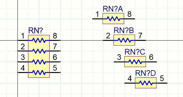
An example with a ganged resistor array (left) and the same resistor array separated into multiple parts (right) is shown below.

For example, take a look at the 6-circuit inverter component shown below. This component contains 6 separate circuits with common power and ground connections. This means we could theoretically create 6 separate symbols for this one integrated circuit (1 symbol for each inverter).
If we want to use a multi-part symbol for this component, we would need to create the following:
- 1 part with 4 pins (VCC, GND, 1 input, 1 output)
- 5 parts with 2 pins (each with 1 input, 1 output)
By doing this, you can place each inverter in a different part of the schematic, rather than routing all circuits into one area of the schematic. This approach is not required, but it is a convenient way to keep a schematic organized. You can even place the different portions of the above symbol into different schematic sheets, which further helps you organize the schematics in your design.
Example: 74LS04
In the example below, we will use a gated component as an example for building the multi-part component. This same schematic symbol part that you see below, a 74LS04, was also used as an example for the symbol generator. Here we will see what it looks like when broken into its separate gates.
The 74LS04 that we are going to create depicted as a multi-part component
Creating an Altium Designer Multiple Component
The first thing that we will do is create a new component in our schematic by clicking on the “Add” button. Because I already had the 74LS04 built as a single symbol component, I am giving this new symbol the name of 74LS04-1. You will also want to fill out the properties for this new symbol with the Designator as model “U?”, the Comment as “74LS04”, and the Description as “74LS04” as you can see below.
The properties setup for our new component
Now you will want to create the symbol using the same process that you would use for creating any symbol manually. Remember that you are creating an individual gate and not the entire 74LS04 component. When complete, the symbol should look like the image below.
The individual gate of the 74LS04
When you create the symbol make sure that you designate the left pin as an input, the right pin as an output, and use the pin names of “A1” and “Y1” just as you see above. The dot on pin 2 is another option available that we used for that pin. You can use a line to draw the triangular shape of the gate itself.
Now that the symbol has been created, you can see it listed in the schematic on the left side of the image below. At this point, it is still a single symbol component and here is where we will add the gates or multi- to it. Go to the Tools pulldown menu and select “New Part.” Now you will see a little arrow next to the component in the list, and when you click on that arrow, the list will display the new part as you see on the right side of the image below.
Adding to our component in the integrated library
This component has six gates in it and you currently have two (A & B). Add four more new to this component to get the full amount of six gates. We will actually need a seventh gate, but we’ll cover that later.
The next step is to draw the symbols in each of those 5 new parts. You could go through the entire process that you first went through when drawing the initial symbol, but there is an easier way to do this. Simply click on “Part A” to activate it, and then select everything in the symbol editing window. Make sure that all of the lines and pins have been selected, and then use the right mouse button to select copy. Now go to each of the new in this component and paste the symbol image into them.
You’ve probably noticed that the copied pin designators and names are incorrect. There are two ways to correct this, the first is to correct each pin individually in each part. You can do this by first selecting “Part B” to activate it, and then selecting the left pin in the symbol editor window. Right-click the mouse and select “Properties” and change the pin designator and name values as shown in the image below.
Editing a symbol pin
Since you are working in the second part, or part “B”, you can see from the logical diagram of the 74LS04 at the top that the input pin of this gate should be pin “3” and named “A2”. These are the changes that you can see were made in the image above. To continue these changes, you would select the right pin and change its designator to pin “4” and its name to “Y2.” Instead of doing all pins individually, there is another way to make pin changes which is faster.
In the properties panel for the component, select the “Pins” tab and you will see a list of all the pins for all six. Select one of those pins and then click on the edit button on the bottom of the panel. This will open up the “Component Pin Editor” as you can see in the image below. With all the data being displayed in one editor it can be a little confusing, but take your time and you can make all the changes you need.
The Component Pin Editor in Altium Designer
In the list of pins on the left side of the Component Pin Editor in the image above, note that the column is titled “Owner.” This refers to the actual part in the component and is very useful in helping you to know which part is which. You can sort by each column by clicking on the column header and clicking on the individual cells to activate that cell for value changes.
Now we need to add the final part that I mentioned earlier. This component has two pins for power and ground which must also be represented on the schematic. To do this we will create another part in this component even though it isn’t an actual gate. Add another part and draw a new symbol and assign the correct values for its pins according to the image below.
Creating the power symbol for our component
Finishing the Multiple Part Component
With that, you have successfully created a multi-part component in the integrated library. Pat yourself on the back, this is an important achievement. There are still a couple of more things to do in order to finish this component. You will want to assign a schematic footprint to it plus all of the other information that you normally would include, such as data links or simulation models. Once you’ve done all of that, your component should look similar to the image below.
Note the display of the in the small pulldown menu in the properties panel. To access this pulldown menu, make sure to unlock it first by clicking on the small lock image directly to the right of it.
The final finished multi-part component
To learn more, read this page in the Altium Designer documentation.
Creating multi-gated parts for schematics can be complex, but Altium Designer has been created as one of the best design systems available in order to make this task intuitive and user-friendly. There are also many other complex aspects of Printed Circuit Board design that Altium Designer’s PCB design software has simplified as well.
If you would like to find out more about how to create the next level of schematics with multi-part symbols, talk to an expert at Altium Designer.


