65W Single IC LED Driver Project
One of the projects I’m working on for personal use at the moment is a high color rendering index (CRI) LED panel, which I’m aiming to make about 300W. I was exploring options for making a high-performance LED driver pcb that would be quite compact, and while I couldn’t build a 300W single IC LED driver, I was able to design a 65W one that didn’t look like it would melt right through the circuit board.
See more Altium Projects or read more by Industry Expert Mark Harris.
I liked the IC, so I thought I’d create a design around it. In the simulation, a two-layer PCB with just the recommended thermal/ground vias runs with a junction temperature of around 120°C. It’s hot but within the ratings of the IC. Making things better, with a basic 30-40 mm fan blowing over the board on the same suggested minimum copper, I was calculating about 102°C on the junction, which is reasonably better. The IC will shut down at a die temperature of 165°C and will return to operation at 145°C, so ideally, I want to ensure stable operation below 145°C at all service temperatures.
My goal for this project is to build a compact yet high-power driver with the capability of driving at least three 12V fans. One fan will be mounted over the LED driver, and the other two can be used for cooling the LEDs it is driving. A 65W LED panel might not need cooling, but if there is the opportunity to do so, it could significantly increase the lifespan of the LEDs in use. For my actual LED panel, I want to power it from a 48V output 350W power supply, such as those made by Meanwell and Delta. In turn, the input voltage of the driver should allow 43V to 53V to allow a 10% voltage tolerance on the power supply.
The input voltage poses an interesting challenge for running 3 fans that are typically 2 watts each. I’m going to use a relatively new IC and Topology that allows very high efficiency but not very clean output power. This is fitting, as the fans are quite insensitive to ripple voltage, making the IC likely to work out as a cost-effective compact option.
This will also be a nice simple project for examining how to configure PDN Analyser for simulating switched-mode power supplies as well, as I’ve already covered basic setup and analysis of linear power supplies in my Motor Driver with PDN Analyzer project.
As usual, this project is open-source and available on GitHub for you to use as you wish.
Driving the LEDs
The IC I’m going to use for this project is a Texas Instruments TPS92512HV. It’s also available with a more limited input voltage for a lower price than the TPS92512. As I was potentially looking at running 5 of these to drive my LED panel, the liberty of having an external clock source was a nice feature for reducing EMI caused by the drivers running out of sync. I also like the high contrast ratio which the TPS92512HV makes possible, and the ability to set the drive amperage from an external voltage rather than just PWM. For my application, PWM would cause flickering and therefore would not be a viable option.
I feel that the current limit of this tiny MSOP-10 package on an FR4 board is going to be around 1.8A. With heat sinks or a metal core board, it would be possible to reach the IC’s rated current of 2.5A, however, I did not want to have the additional cost of a metal core board for this project. For the board I’m designing, the thermal performance could likely be significantly improved by adding a cheap heat sink under the fan.
If you’ve ever designed a buck-mode switched-mode power supply, you’ll feel right at home with the TPS92512. At a schematic level, it’s just a buck regulator with a current sense pin. There’s much more going on inside the IC than the typical buck regulator, but for schematic design purposes, it’s very similar.
Under Voltage Lockout (UVLO)
The first set of equations in the datasheet is for setting the under-voltage lockout, which seems as good a starting place as any for the design. Unfortunately, the equations seem to fall apart at about 33V. I was able to use the example equations to calculate values for a set of resistors for lower voltages, with results matching the sample in the datasheet, but not for 43V. Based on the sample equation, UVLO appears to trip at around 1.22V, so I simply calculated a resistive divider for this voltage and will make any changes required after investigating how these values work in a physical prototype.
We’ll circle back to this later on in the article, as requiring the fans to be operating introduces an interesting need to turn off the LED driver if the 12V power supply is not operating.
Adjustable Switching Frequency
The TPS92512HV can have a switching frequency between 100kHz and 2MHz, which is a very broad range allowing for it to be used in a variety of solutions. At the same time, it also means more design work for me! I need to work out a frequency that will allow me to use small enough components, but also be highly efficient. There are some limitations on the frequency placed by my high input voltage, which makes life easier.
I ended up settling on a frequency of 345kHz for my implementation, set by a 348k ohm resistor.
Inductor Choice
The datasheet contains clear formulas to determine both the inductance and the current ripple through the inductor to allow the selection of an optimal inductor. Beyond these values, you also need to take into account the DC resistance (DCR) of the inductor, which will have an impact on heat and efficiency.
Given that my project’s fan will be the largest component—which will be a limiting factor as far as size—I decided to go with an inductor that is significantly larger than the minimum possible footprint. This will help keep temperatures down, and slightly increase the efficiency of the driver. I am using a TDK SLF12575T-330M3R2-PF, a 33uH inductor, which is not the lowest DC resistance option out there in this amp range but is at about half the price of options offering lower DC resistance, making it a good tradeoff between resistance and cost.
Capacitors
The datasheet has suggestions for the minimum capacitance required for the stable operation of the device, but I’m a fan of overdoing things. The board itself will have a nice big input capacitor, which will help the AC-DC switched-mode power supply deal with any rapid fluctuations in demand from the driver, as well as potentially reduce EMI transmitted from the board. I’ll also provide around 5 times the recommended input and output capacitance to the IC to ensure stable operation. Increasing the capacitance barely adds any additional cost to the board, so in my opinion, there’s not much reason to skimp. If I was making millions of these, where cents added up to real money, this decision might have gone a different way.
Rectifier Diode
The rectifier diode is going to have a decent amount of power to dissipate. A diode with low forward voltage and a large package size is good here to ensure the area around the IC stays as cool as possible. The larger diode package gives larger pads to conduct heat away, as well as more surface area to cool down under the fan, and the lower forward voltage reduces the power dissipated in the diode proportionally. Comparing an SMC package with an SMA one, the diode is almost 20°C cooler with the larger package option, which is considerable.
Current Setting
I’m using a 150-milliohm current sense resistor to get close to the 300mV of voltage drop at full current that the datasheet suggests. As I can’t quite get to 300mV with standard values, I will need to make my voltage divider for the IADJ pin give me something a bit lower than 1.8V. With 271mB of drop on the 150-milliohm resistor, I’ll need 1.626V on IADJ to get my maximum drive current.
LED Driver Schematic
The LED driver schematic
We now have the driver schematic calculated. I’ve also added a ferrite bead to the input voltage, as all switched-mode power supplies like to make a lot of noise on both the input and output. D1 is for clamping the output voltage to not rise higher than the input voltage, which could otherwise have been caused by ringing between the inductor and output capacitor. There’s also a connector in the top right with a basic current limiting resistor on it to protect any devices that are controlling the driver’s PWM port in the event of a catastrophic failure of the driver IC. The 1K resistor to ISENSE serves a similar purpose, preventing the IC from being a conduction path to ground in the event of the current sense resistor failing.
Powering the Fans
To supply power to the onboard fan, and up to two others, I’m going to use the Texas Instruments LM5166 buck converter. This will sufficiently handle my 500mA of load and has a high enough maximum input voltage. The constant on-time buck converter allows for a very high-efficiency design in a compact space, however, it does require an output voltage ripple far more substantial than most regulators to function. If this device was used to power a microcontroller or some other sensitive device, it would need to supply a linear regulator for the final output voltage to provide a smooth, low noise supply. For powering a fan, however, it’s going to be a great option, taking up very little space on the board.
The design process for the voltage regulator is quite similar to the LED driver, as both are operating as buck regulators. Other than the current sense resistor to the LED driver, the voltage regulator has one major difference: the ripple generation network.
Ripple Circuit
For this regulator, I’m going to go with the basic type 1 ripple circuit for simplicity. However, if you planned on implementing this in your design, I’d suggest taking a look at a type 3 ripple circuit that’s a bit cleaner and has lower noise. There’s a great white paper on this here. When designing most voltage regulators, my goal is to remove as much voltage ripple as possible from the output, so it feels a little strange to deliberately design a circuit to cause a ripple. Having a resistor in series with your output capacitor feels very wrong, but that’s precisely what this design calls for!
My design will have a 1.1-ohm series resistor with 22uF of capacitance on the output. This should produce the required voltage ripple for the regulator to function as a constant on-time supply.
Ensuring the LED Driver Stays Cool
As I mentioned earlier, I want to make sure that the LED driver won’t run without an operational 12V supply. Without the 12V supply, there is no cooling and this could be catastrophic to the board if it’s operating in an elevated temperature environment.
To do this, I am going to use the power good output pin from the 12V regulator to control the undervoltage lockout pin of the LED driver.
When the transistor is ON, UVLO will be the midpoint of the voltage divider between R4 and R8.
I’ve added a MOSFET to the voltage divider for setting the minimum input voltage for the undervoltage lockout feature on the LED driver. This is then connected to the power good output from the voltage regulator. If the voltage regulator does not output the power good signal, then the UVLO pin on the LED driver will only see a 1.54k pull-down resistor, which will ensure the driver stays off.
12V 6W Power Supply Schematic
The schematic for the 12V power supply using the TI LM5166
The schematic of the 12V power supply is fairly simple. Once again, we have a ferrite bead on the input to mitigate any potential EMI issues that could cause a certification attempt to fail. I’ve also added a small LED, which the 12V power supply will light to show that the board is powered, and I’ve also added 3 output connectors.
Reverse Polarity Protection
My preferred method of adding reverse polarity protection is using a reverse-biased MOSFET. Using a MOSFET results in a very low voltage drop, and a very small amount of heat generated. You can use a MOSFET to provide reverse polarity protection for a relatively low current board such as this, but I’ve also used them on boards that handle over 100A.
For this board, I’ve added a voltage divider to the gate of the MOSFET, as it’s difficult to find an affordable, compact MOSFET that can take 48 volts or more on its gate pin.
The behavior of the circuit in reverse polarity is elegantly simple: the MOSFET is essentially in the circuit backward, allowing current to flow through the body diode when the circuit is correctly polarized. This small current allows the gate pin to function, which allows the MOSFET to conduct current normally through the junction.
The transistor here acts as a low voltage-drop reverse polarity protection device.
This was my original schematic for the reverse polarity protection, and it’s wrong. I didn’t discover my mistake until I was routing the PCB. While the circuit is protected from the input being reverse polarized, the two small electrolytic capacitors are not. Electrolytic capacitors don’t fare very well being reverse polarized, so a change needs to be made to their connections.
The negative terminals of the capacitors are now connected to the ground instead of to the transistor’s source pin
This is the correct way to protect the entire circuit, including the two capacitors!
Other Schematic Items
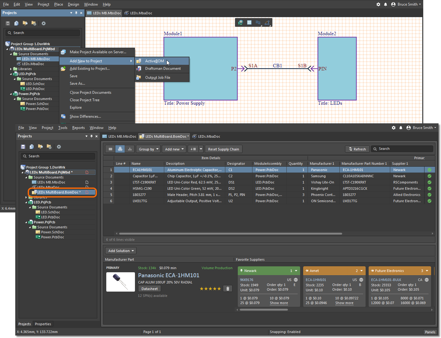
I’ve also added fiducials, a relatively quiet 40mm fan, and M3 standoffs to the top sheet of my schematic. Adding the mechanical components (such as the fan and standoffs) to the schematic sheet puts them in the BOM document too. That way, I can be sure I won’t forget to purchase them when ordering the other components. This also gives me more accurate pricing in the ActiveBOM extension without needing to manually add rows to the document. The fan and standoffs are sourced from electronics suppliers, so they should also have substitute parts available in the ActiveBOM to allow for the cheapest option to be ordered for any particular purchase volume.
Board Layout
As usual, we start with an engineering change order to add all the components from the schematic to the circuit board. I’ve covered my process for using cross selections and the Arrange Components Inside Area tool to quickly separate components into logical blocks and lay them out individually in my other projects. If you’re interested in how I quickly lay out components on a board, you might want to consider taking a look at my Sub 1GHz RF Transceiver project.
As in my Sub 1GHz RF Transceiver and other projects, I start by laying all the components out off-board
12V Power Supply
The schematics above for the 12V power supply are the final version, with just one output capacitor. Originally I had designed the supply using 3 smaller capacitors, yet during the PCB layout, I found this was not a wise decision.
The original three-capacitor setup turned out to take up too much space.
This is because the inductor for the 12V supply should be as close to the IC as possible, and with 3 capacitors, this was not going to happen.
The PCB layout for the three-capacitor schematic above.
By using a larger footprint, and a higher capacitance part, I was able to achieve a much better layout that will perform better.
In the new schematic, the IC is a lot closer to all of the components connected to it.
The components should be placed as closely as possible to the regulator IC, and the datasheet has excellent guidance on the suggested layout for this IC if you haven’t worked with switched-mode power supplies before.
Component Clearance Rules
When placing the fan on the standoffs, Altium Designer quickly informed me of a clearance issue between these parts, as the default constraint allowed for a minimum clearance of 0.254mm. I created a new clearance rule for the 40mm fan to M3 standoff, to allow the fan to sit directly on the standoffs.
A component clearance rule allows components to sit above each other.
I have to admit, this is a feature of Altium Designer that I find extremely useful. My library has full 3D models for every component, which allows me to place overhanging connectors such as the one shown in the rule picture over small passives without worrying about assembly problems. If you have good 3D models in your library, it becomes a very powerful check of your design.
Once my clearance constraint was corrected, I added the fan and the standoffs to a union (Tools -> Convert -> Create Union from Selected Objects) so they would move together as I figured out the placement of all the parts on the board.
Overall Layout
I now have the board at a point where everything fits together nicely under the fan, without adversely affecting the efficiency of the power supply routing. My input power is on the left side, and the LED connections are on the right side. The board could be significantly more compact if there wasn’t a fan which requires mounting holes, but this configuration allows more heat dissipation and is therefore preferable to a compact design. Coupled with an enclosure with intelligent air vent locations, this should drive airflow over the components and board keeping everything at a reasonable temperature.
The final component layout is yet to be routed.
With the general layout complete, I like to first route the higher current portions of the board. With switched-mode power supplies, I like to route using polygons rather than tracks. By using polygons, I can keep the current densities low as well as maximize the area for thermal performance. As this board is just two power supplies, it’s almost completely routed using polygons!
The layout above after polygons to route the two power supplies was added.
It’s easy when designing a board like this to get a little carried away with the polygon sizes, and completely forget about the ground pads of the components both for thermal and electrical conduction. Therefore, my next step is to route the GND net using traditional traces of any width. The top layer will have a full ground pour, but I want to ensure that electrical paths are going everywhere they need to. By manually routing a trace where I want current to flow, I can ensure I don’t end up with any islands or odd current flow routes once the polygon is poured.
The final power supply routing.
The only unrouted nets now are signals such as the power good output from the 12V regulator, and the PWM input. I was going to make this a two-layer board, but I want to keep the ground pour on the bottom of the board unbroken for thermal reasons. As such, I’ll go with a four-layer board and use one of the internal layers for the signals. The internal layers are great for signals, as most low-cost manufacturers will make these out of thinner foil.
The layer stack up
Despite the inner layers are not of much use for thermal purposes, as they are insulated by the core and prepreg on either side, I’ll have to use my ‘spare’ inner layer as a ground plane too.
If you’re new to Altium Designer, or upgrading from AD17 or earlier, you can set the plane’s net by double-clicking on it.
With the polygon pours on top, the board is looking pretty good! Each power supply exposed pad has a decent thermal path out to the plane while also having a sufficient copper area for the other components as well.
After adding the polygon pours to cover the entire area of the board.
Currently, the design is still missing a lot of vias. We need vias around the regulators to help conduct both heat and current to the other layers. I’m also adding some relatively large (1.5mm) vias to act as a crude heat sink. In previous designs, I’ve found this to be about the minimum size to allow enough air through the holes to function as a heat sink with low-pressure forced cooling.
After adding a lot of vias to conduct heat.
Because I intend to have this design in an enclosure, I removed the solder mask from around my crude heat sink holes.
I had a long discussion years ago with a mechanical engineer friend about whether a black solder mask (i.e. black body) would radiate more heat, or whether the solder mask would insulate the copper so less heat would be radiated/convected. We didn’t come to a sensible conclusion, so I’ve continued removing the solder mask on enclosed PCBs where I want more heat to escape. If you have an opinion one way or another, please leave a comment. It would be great to see what others think.
Final 3D render of the top of the board in Altium Designer
In 3D, the board is looking pretty good! The fan should provide good airflow over the components that will get the hottest. With an enclosure to direct air down to the LED connector end of the board, it should provide even more airflow over the hottest areas.
For the bottom of the board, I removed the solder mask from the areas that will get the hottest as well, while ensuring I left vias that are not connected to the GND net covered with mask/tented.
Final 3D render of the bottom of the board in Altium Designer
The Enclosure
In my last project, I thought it would be fun to have an enclosure made by a freelancer just to finish the project. The results were more than I had hoped for, so I’ve returned to the same Danish freelancer to make a case for this project. The enclosure will ensure the airflow goes where I want it and make the project look a little more stylish when assembled.
The final product is rendered with a beautiful enclosure.
I had some ideas for the design, primarily related to venting locations. I wanted to ensure that there would be vents below the board to ensure there wouldn’t be a pocket of hot air trapped under the board, and I wanted the top vents to only be at the LED connector end so air from the fan would travel down the board before exiting. Other than that, I mostly left it up to William to decide what to do for the design. Once again, I’m very pleased with the style of the enclosure; it's a lot more aesthetically pleasing than a typical electronics box!
The enclosure is capable of being injection molded with just a basic two-part mold and is small enough for me to fit into my resin printer for prototyping, testing, or low-volume production.
He offered me a range of renders in different colors, but the blue looks pretty fun to me! The black option is fairly serious looking, which makes me ponder how significant an impact just changing the color of the plastic on an enclosure has on the feel of the product!
Which looks better, the fun-looking blue or the serious-looking black?
Using This Design
This design is released as open source on GitHub. You can download the project yourself and use the design files as you wish.
What's Next?
In the next article, I’m going to look at doing some simulations on this design to see how well I’ve done with the layout! I’ll use the PDN Analyzer addon to build a simulation including the switched-mode power supplies and make sure there won’t be any spots on the board with excessive voltage drops or current densities. When designing voltage regulators or drivers, PDN Analyzer can provide impressive insights into the functionality of the design.
See more Altium Projects or read more by Industry Expert Mark Harris.


