It’s All Analog
“It’s all analog!” I would state emphatically, often banging the table for effect. Those in the room that knew me would continue working, those that didn’t believe me could be seen to roll their eyes, but sometimes I would get the attention of a new hire or someone just out of school, and they might ask “what about digital?”
The time was the middle of the 1980s, and I was working at Commodore Business Systems as a senior design engineer, which meant my mistakes got reproduced in the millions. I had never been to college and had come up through the ranks starting as a licensed Television repairman. To say I was self-taught would not have been quite true as once I got into various engineering departments I learned from the brilliant people around me. I also made a point to learn from mistakes, whether mine or theirs.
If we skip the point in time inhabited by the “ECL Generation”, the subsequent “TTL Generation” had the temptation to think in terms of digital connotation, namely they get to call signals “high” or “low”, or for even shorter words, a “1” or a “0”. Simple right? Of course, now we know and use terms like Signal Integrity (SI) and Power Distribution Network (PDN), but back then processors in consumer and small industrial equipment were relatively new.
Suddenly we had a generation of new engineers that “did digital, but not analog”. I would come to find out that most of them meant they didn’t do ground loops, FCC emissions/susceptibility, power supply design and even reset circuits were outside of their comfort zones. Personally, I saw the job as being all-encompassing, a prime example being that the first thing I taught any properly schooled engineer that joined my ranks was how to calculate what the junction temperature of a chip would be.
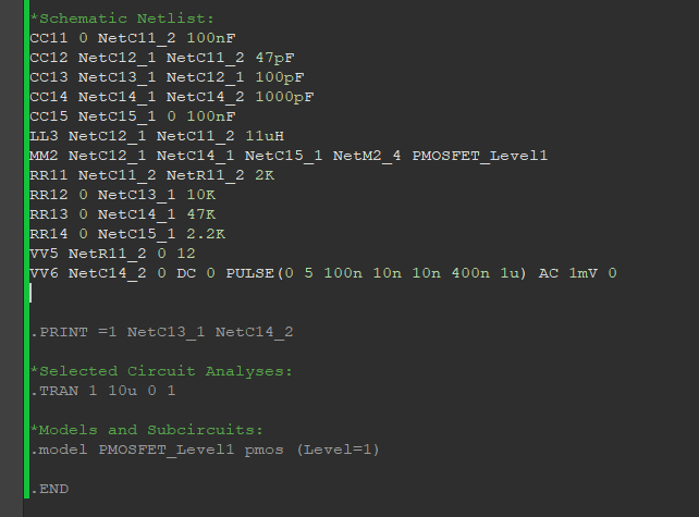
Case in point, when I got to Commodore I found that the proposed reset circuit, for what would become the C116/C264/Plus4, was comprised of a circuit in which someone had hooked a capacitor to a resistor to the +5V supply to the input of a gate. I got very vocal in my declaration that this simply would not work. Picture a long-haired kid with no schooling telling you this on his first week working there. At least I hadn’t started taking off my shoes at work yet.
So the engineer, it turns out the outgoing engineer as he was moving on to less stressful surroundings, patiently explained that the founder of the company had set a limit on the number of chips that could be in the new computer, the number was nine. I patiently explained that that didn’t matter and that the circuit wouldn’t work. Commodore’s response was to make me in charge of the new line of computers and now it was my problem. I added a dedicated reset circuit on the form of a 555 timer chip and the founder did not fire me, at the end of the day we needed it to work at every quantity, low and high.
Fast forward ahead to my latest tirade; I was in charge of the Commodore C128’s design and hardware, and had to put a dual-processor system—with dual graphics processors and a total of 144mB of DRAM—on a 2 layer board, and have it work in the quantity of millions (and it’s 1985). At the heart of the problem is that most designers can get away with something that works 95% or in most voltages or combinations of chips, but a million times a 2% problem is an awful lot of machines sitting on skids and in scrap piles. These numbers can and will exercise the problems of sensitivity to chip brands and variations and every combination of temperature and voltage.
I worked hard to impress upon anyone who would listen that what they called a “low” was really a threshold voltage of .8V as seen by the chip when the driver chip might have as high an output as .4V, leaving a paltry .4V for noise margin. We used to joke that OR gates were “noisier”, as any spike of greater than .4V on either input could cause the output to start to become invalid.
To compound the difficulty in what we were doing is the fact that we never ever thought to use a multilayer board in the consumer division, not once, not ever. That meant that our power traces were nothing more than bigger signal traces by today’s standards, and the impedance of both power and signal traces varied widely based on the luck of the layout.
These were the days before any practical tools for predicting bad behavior; consequentially we just assumed the behavior would be bad. Even the IC designers did not have the tools that told them if the chip matched the schematic, only building the chip and testing it would provide the ultimate answer. So too for the systems, we had to build them to see what we had.
I had two tenants when starting a new design; the first was to grid all power and ground, all chips should have two paths to both power and ground, which meant in theory that there would be no stubs. The second was really a starting point, and that was to place and route the DRAMs which were by far the trickiest beast of the day. Not all DRAMs were made correctly, not all power supplies held their tolerances (DRAMs are voltage-sensitive in some aspects), and the very chips that created the timing had issues. Our one edge was to try to make sure that the power PCB layout did not also contribute to these issues.
Next, we would instantiate the graphics chips, which included the master clocks—the highest fundamental frequencies on the board. We automatically designed for a small shield to encase this part of the design, our sinning had begun and so had the patching-over of those sins.
When done, we would generally have a mess by today’s standards, and again our test was not whether we could produce a few, or a few thousand. A million was the minimum and generally, we ran over five million.
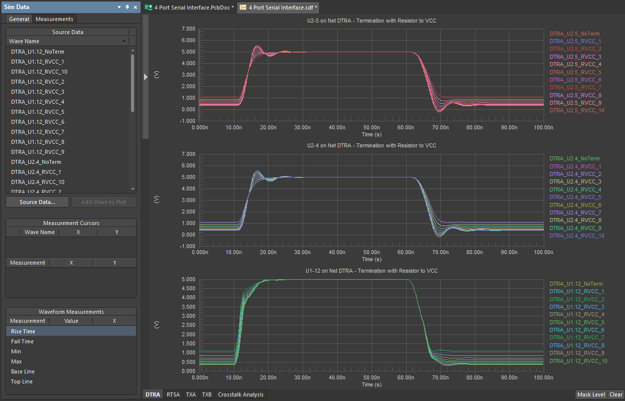
Getting back to highs and lows, the signals back then could ring like bells or show up with half a dozen reflections or crosstalk it had picked up along the way. There was no more room on the board for grounds or shields or separation and there was no more time in the schedule to ”start over” in any significant way. This meant we had to understand and adapt to our environment. Sad to say, that what we then did was “tune” the mess so that it would appear to operate properly. We lived with artifacts as long as they settled down during critical times such as DRAM control signal transitions.
One thing we would do was reach for series termination by the handful. We tried ever to value-up to 68 Ohms but the sweet spot for us was typically 22 Ohms, 33 Ohms if we had time for the extra RC component. I also found several instances of ground lifts and also had to manually tune an address line by adding a discrete wire: to 5.7 million units.
I showed the newly arrived “digital” engineers that you couldn’t count the time a signal spent ringing as either a high or a low until it stopped ringing. Suddenly, analog had entered their digital view of the world as I forced them to redo their timing calculations based on real-life artifacts. “It’s all analog”, I would state loudly until one day a fellow engineer named Hedley asked, “What about quantum effects?”
After that my motto became “IT’S ALL ANALOG… until of course, you get down to quantum effects in which case it’s not”.
Would you like to read more inspiring stories about technology? Read articles in the Altium OnTrack Newsletter, curated by Judy Warner. Or find out more about how Altium can help you with your next PCB design and talk to an expert at Altium about the applications of printed circuit boards and using the only unified PCB design software package on the market.


