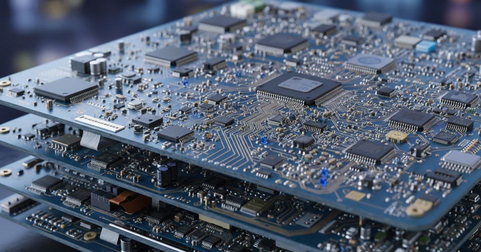
Electromagnetic Interference (EMI)
Explore how smart PCB design minimizes electromagnetic interference and ensures compliance with EMC standards. From grounding techniques to layout strategies, these resources help you build quieter, more reliable electronic systems.
Migracja z Allegro
Explore Guidebooks for Electromagnetic Interference, EMI and EMC and start creating today!


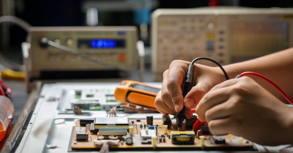
Technical Documentation
Explore Technical Documentation related to EMI / EMC

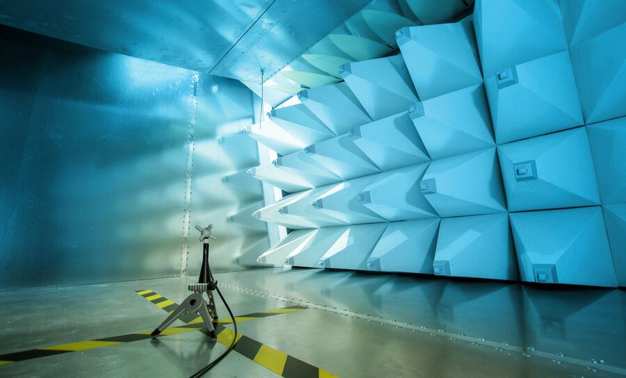
Articles
Explore more popular content for Electromagnetic Interference, EMI and EMC!